What is a semiconductor?
Semiconductors are the key enabling components used in the electronics industry today. Electronic components based on semiconductor technology include ‘discrete components’ including many different types of transistors such as bipolar transistors or MOSFETs, or diodes such as light-emitting diodes (LEDs), and an ever-expanding range of analogue and/or digital ‘integrated circuits’ (ICs). Unlike discrete semiconductor components, integrated circuits can include literally millions of transistors in large microprocessor chips, for example. Strictly speaking, a semiconductor is not a component but actually a material such as silicon. Silicon is the dominant material used in the industry today, but there are many others including germanium for example. A semiconductor is somewhere between being an excellent conductor such as copper and an excellent insulator such as plastic or glass. It therefore will sometimes conduct electricity, depending on electrical stimulation in a specific direction. It is therefore an excellent material to be used as an electronic switch, assuming it is required to perform in this way, either conducting or not and thereby providing the ‘1’s or ‘0’s required in binary computing and digital processing based systems, for example.
What is a diode?
A semiconductor diode is a basic semiconductor component and was the first available semiconductor-based electronic device. A diode is a semiconductor that has a ‘p–n junction’ connected to two electrical terminals. The p–n junction is an elementary ‘building block’ used in most semiconductor devices including diodes and transistors. A p–n junction is a boundary or interface between two types of semiconductor material: p-type and n-type, which are created by implanting impurities.
The diode features ‘asymmetric’ characteristics: it has low (and ideally zero) resistance to current flow in one direction, and high (and ideally infinite) resistance in the other direction. The non-linear current–voltage characteristics of diodes can be further adapted by the use of different materials and by adding impurities into these materials, also called doping, to allow them to perform different functions.
The most common function of a diode is to allow an electric current to pass in one direction (forward), while blocking current in the opposite direction (reverse). The diode is commonly used in electrical circuits, such as in a diode bridge, to ‘rectify’ a signal to convert alternating current (AC) to direct current (DC). In addition, diodes can also be used to conduct electricity only if a certain threshold voltage is present in the forward direction (or forward-biased). The voltage drop across a forward-biased diode will vary only slightly with the current, affected by temperature. This effect means that a diode can be used as a temperature sensor, for example. A range of different types of diodes (described below) are available including PIN, constant-current, TVS, Zener, Schottky and rectifier types.
What is a PIN diode?
A PIN diode is a type of semiconductor diode that has a wide and very lightly doped region in between the p-type and n-type regions. This wide ‘in-between’ region, in contrast to an ordinary p-n diode, makes it suitable for use as a fast switch or an attenuator* in high-voltage power electronics, rather than as a rectifier.
Key attributes for PIN diodes include:
- Diode configuration including single, dual, common cathode or common anode - Target applications including attenuators or switches - Operational frequency range such as VHF, UHF or SHF - Forward conduction current (max) - Forward voltage (max) - Reverse voltage (max)
What is a constant-current diode?
A constant-current or current-limiting diode comprises a junction gate field-effect transistor (JFET)* with the gate shorted to the source. It functions like a two-terminal current limiter, allowing the current to flow only up to a certain value and then level off at a specific value.
Key attributes for constant-current diodes include:
- Diode configuration including dual or common anode - Current (max) (where voltage is less than the peak operating voltage) - Current limiting break-down voltage - Constant-current-limited voltage (max)
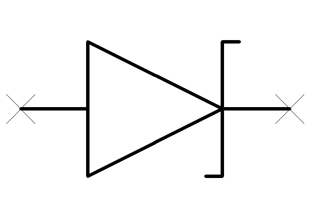
What is a TVS diode?
Transient-voltage-suppression (TVS) diodes are used to protect electronics from transient ‘over-voltages’ or voltage spikes. The device ‘shunts’ excess current when the voltage exceeds the avalanche breakdown potential, thereby suppressing all over-voltages above the breakdown voltage. Generally, a TVS diode will respond to over-voltages faster than other over-voltage protection components such as varistors.
Key attributes of a TVS diode include:
- Device configuration including dual or common anode - Voltage at fully rated current - Pulse current (max) - Conduction voltage - Current limiting break-down voltage - Zero-conduction voltage threshold
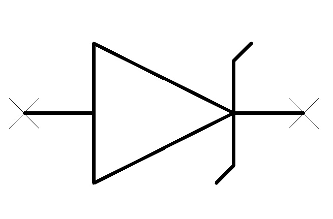
What is a Zener diode?
While the common diode allows current flow in one direction only, the Zener diode tweaks this rule. While it allows current to flow in the forward direction in the same manner as an ideal diode, it will also allow current flow in the reverse direction when the voltage is above the breakdown voltage. The Zener diode is commonly used to provide a reference voltage for voltage regulators or to protect other semiconductor devices from transitory voltage pulses.
Key attributes of a Zener diode include:
- Device configuration including dual or common anode - Type of Zener, including Avalanche Zener or voltage regulator - Voltage tolerance - Voltage drift with temperature - Impedance (max)
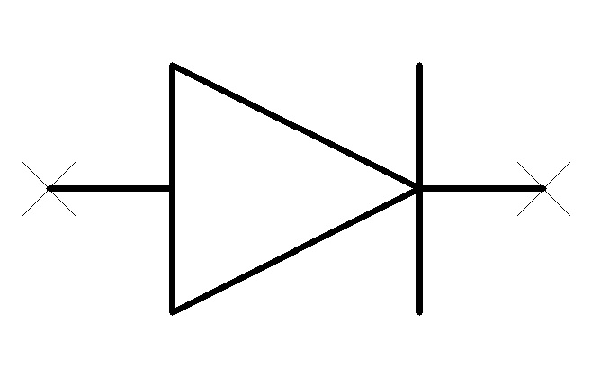
What is a rectifier diode?
While rectifiers may be used in many types of circuits, its primary mission is to convert alternating current (AC) to direct current (DC), which is known as rectification. Rectifiers are most often used as comonents of AC/DC power supplies and high-voltage DC power transmission systems. The opposite of a rectifier is an inverter, which implements more complex circuitry to perform conversion from DC to AC.
Key attributes for rectifier diodes include:
- Type of circuit, such as switching diode - Device configuration including single, dual, common cathode or common anode - Continuous current (max) in forward direction - Reverse voltage (max) that is sustainable without damage - Forward voltage (max)
What is a transistor?
The transistor is the essential component of all modern electronic products. This elemental device can be found in all electronic systems. Transistors can be packaged individually as ‘discrete components’ or integrated in quantities of hundreds, thousands or millions in integrated circuits such as microprocessors. Its continually decreasing size and the ability to achieve higher levels of integration has led to a transformation in computing power over the past 60 years or so.
The transistor essentially has two basic capabilities: it regulates current or voltage flow and can be used to ‘amplify’ and/or ‘switch’ electronic signals and electrical power. It is built from semiconductor materials and has at least three terminals for connection to an external circuit. A voltage or current applied to one pair of the transistor's terminals changes the current through another pair of terminals. A transistor can amplify a signal because the controlled (output) power can be higher than the controlling (input) power.
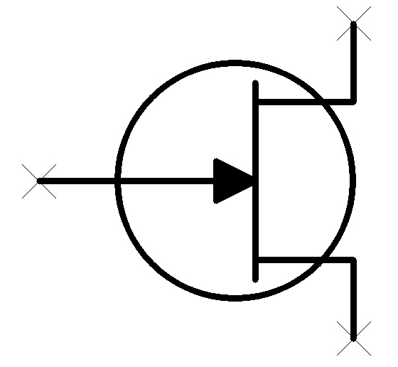
What is a bipolar transistor?
The bipolar transistor, also known as a bipolar junction transistor or BJT, is a type of transistor that comprises two p–n junctions in series, implemented as either n–p–n or p–n–p types. Bipolar transistors are commonly used for amplification of either analog or digital signals, in addition to be used as switches or in oscillators. They are commonly used as individual discrete components or in huge quantities within ICs.
Contacts are made to all three regions: the two outer regions are the emitter and collector and the middle region is called the base. A bipolar transistor amplifies current, but it can be connected in circuits designed to amplify voltage or power. The collector-emitter current is essentially controlled by the base-emitter current (current control) or by the base-emitter voltage (voltage control).
Key attributes for bipolar transistors include:
- Transistor type, such as n–p–n or p–n–p - Transistor configuration, such as dual or common base - Number of transistors per device - Collector current (max) - Collector-emitter voltage, VCE (max) - Power dissipated (max) - Current gain (min)
![]()
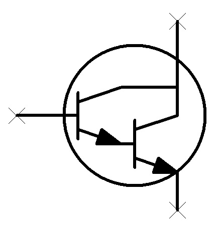
What is a Darlington Transistor?
The Darlington Transistor, or Darlington pair, comprises a pair of bipolar transistors. These can be either integrated in a single device or discrete devices can be connected in such a way that the second transistor will further amplify the current that has already been amplified by the first transistor. This configuration gives a much higher common/emitter current gain than each transistor taken separately. Integrated Darlington pairs are available in standard discrete packages or as an array of devices in an IC.
Key attributes for Darlington transistors include:
- Transistor type, such as n–p–n or p–n–p - Transistor configuration, such as dual or common base - Collector current (continuous) (max) - Collector-emitter voltage, VCE (max) - Base-emitter voltage under saturation, VBE(sat) (max) - Current gain (min)
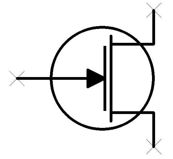
What is a JFET?
The junction gate field-effect transistor is the simplest type of field-effect transistor (also the basis of the MOSEFT) and is used as a switch or voltage-controlled resistance. Charge flows through a channel between the source and drain.
Key attributes for JFET transistors include:
- Transistor type, such as n–p–n or p–n–p - Device configuration, such as dual or dual-drain - Drain current (continuous) (max) - Drain-source voltage, VDS (max) - Gate-source voltage, VGS (max) - Gate-drain voltage, VGD (max)
What is a MOSFET?
The MOSFET (Metal–Oxide–Semiconductor Field-Effect Transistor) is a transistor used for either amplifying or switching electronic signals. Although the MOSFET is a four-terminal device with source, gate, drain, and body terminals, the body (or substrate) of the MOSFET is usually connected to the source terminal, making it a three-terminal device. The MOSFET has become the most common transistor used in both digital and analog circuits.
The MOSFET has better switching performance than the bipolar transistor. It is a voltage-controlled device, which requires negligible power to sustain conduction, meaning power savings over the bipolar transistor. In highly integrated components, MOSFET transistors are used in CMOS (Complementary MOS) technology, with significant size scaling meaning that millions of these devices can be integrated in ICs.
Key attributes for MOSFETs include:
- Transistor type, such as n–p–n or p–n–p - Drain current (continuous) (max) - Drain-source voltage, VDS (max) - Gate-source voltage, VGS (max) - Drain-source resistance, RDS(ON) (max)
What is an IGBT?
The IGBT (Insulated Gate Bipolar Transistor) is essentially a power transistor switch that offers high efficiency and fast switching and is widely used in power electronics applications in motor control, lighting and many others in industrial and consumer sectors. The IGBT has high input-impedance and low output-impedance characteristics and combines the advantages of power MOSFETs and bipolar transistors, delivering a large current-carrying capability like a bipolar device but with the ease of control of a MOSFET.
Key attributes for IGBTs include:
- Device configuration such as dual or array - Transistor type, such as n–p–n or p–n–p - Collector current (continuous) (max) - Collector-emitter voltage, VCE (max) - Gate-emitter voltage, VGE (max) - Switching speed (max)

What does packaging mean?
Discrete semiconductors are supplied in packages (usually plastic, ceramic, metal or glass), which protect the semiconductor material (usually silicon). The package provides protection and holds the contact pins or leads or pads used to connect the device to external circuits. The package is also important in dissipating heat produced in the device. There is a wide range of different semiconductor packages available, and the choice will depend largely on size, lead/pad count and power dissipation among other characteristics.
In general, there are packages for through-hole technology, where components with wire pins or leads are fitted through holes in the printed circuit board (PCB), and packages for surface-mount technology, which is an excellent low-profile space-saving method where components are mounted directly on to the surface of PCBs connecting via pads or balls.
In addition to the above, special devices also exist, such as LEDs (light-emitting diodes) or light-sensing devices for example, which will require a ‘window’ in the package.
Glossary of other terms Attenuator – A device that reduces the power of the signal without appreciably distorting the waveform. PCB – The Printed Circuit Board is a non-conducting board or substrate that is used to connect electronic components, such as discrete semiconductors or ICs, or passive devices such as capacitors, inductors or resistors, via conducting copper tracks to make an electrical circuit.