Getting Started
Power supplies generate noise that can reduce the performance of a design and interfere with other devices. Signals themselves can interfere with each other and reduce the performance of the system.
Knowing how the system functions, where the noisy lines are and where the sensitive lines with a low signal to noise ratio are in relation to each other can help optimise the board layout and avoid more problems later in the design. EMI can be treated later on by adding filters at noisy points, or using metal enclosures that block radiation, but these can be expensive options and add time and cost to the development process through more testing and re-spins of the board. With edge effects and connectors being a key part of the EMI issue, these re-spins can even involve moving key I/O lines. Taking EMI effects into account at the start of the board design can significantly improve the quality of the end product and avoid any nasty surprises.
Power supply
The board layout determines the success or failure of every power supply project, from the function to the EMI and thermal behaviour. The design of a switching power supply layout is not difficult but it is often left until too late in the design process.
A good layout on the first prototype does not add to cost, but actually saves significant resources in EMI filters, mechanical shielding, EMI test time and PCB runs. Switching supplies can radiate at frequencies that are very obvious, affecting nearby radios, but good layout can avoid the need to shield such systems.
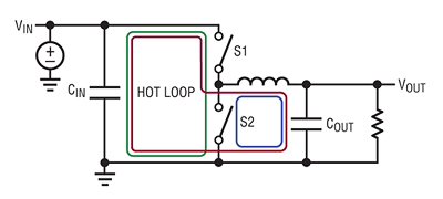
The EMI problems come from fast changing current loops, so avoiding these hot loops or making sure they are not fast changing can make all the difference in the design. Different power supply topologies such as buck or flyback converters create different AC loops, but carefully positioning these, sometimes within the layers of a board, can help significantly. This helps to shield any radiating effects and minimises the need for filtering or expensive metal enclosures. Making sure these loops are away from the vias that connect the different layers and away from sensitive lines with low signal-to-noise ratio also helps reduce the impact the power lines have on the rest of the system.
Signal lines
The biggest problem for the signal lines is the noise from the I/O pins, which often form a large antenna. In a synchronous design, all the signal switching happens on the same edge and this can create a large noise spike at regular intervals. With the clock rates increasing, these signals become more important to address in the board design.
Capacitive and inductive crosstalk happens with traces that run parallel for even a short distance. The noise is proportional to the parallel distance, the frequency, the amplitude of the voltage swing on the source, and the impedance of the victim, and inversely proportional to the separation distance.
This can be minimised by keeping noisy lines away from more sensitive traces and by avoiding running noisy traces on the outside edge of the board. Keeping noisy traces grouped together surrounded by ground lines will also help to reduce noise as any coupling is to ground rather than to other signal lines. This can be particularly important for the I/O lines where switching generates noise and can radiate out of the system. Signals that may become victims of noise should have the return ground run underneath them. This reduces the impedance, reducing the noise voltage and any radiating area.
Clock tree
A third source of noise is the oscillator circuit, where the oscillator swings rail to rail. In addition to the fundamental frequency, harmonics are introduced on the output side. Keeping the crystal and its tank circuits separate from other components and traces on the PCB, and keeping the loop areas small usually avoids this problem and prevents signals from coupling into other components such as large inductors.
Many EMI-related crosstalk problems happen around the crystal, so keeping a minimum separation of at least 2cm between the oscillator and other components helps to reduce any sensitivity. This usually happens as part of a zone (see below).
Radiating antennas
Any trace that is around 8cm or longer that is unterminated forms an antenna that radiates in the FM band. This is easily addressed by avoiding long signal lines and terminating them with a series resistor to provide damping without slowing down the data transmission. This is where the layout of the board feeds back into the netlist in an iterative process.
Lines that bend too sharply can also radiate from the corners, so the design tool rule checks should flag up where there are sharp bends. These corners are also risk factors for the yield in the manufacturing process, so avoiding them gives additional benefits.
Zones
Creating zones of similar functions can help focus the requirements for the board layout. Keeping all the analogue elements in one area, shielded by a split ground plane or with ground lines designed to protect the zone from the power or digital circuitry, can reduce the sensitivity of the design to coupled noise. This also allows more time to be spent on designing the analogue area of the board, while the digital elements are less sensitive to noise. Similarly keeping the power components in one area of the board, well away from other sensitive components can also help.
Auto routing
While an automated routing tool may seem helpful, taking these factors into account and constraining the tool can help. Providing automatic routing within zones on the board can help speed up the layout process while at the same time minimise the impact of EMI in the design. Auto routing may not pick up on long signal lines or noisy lines that run alongside susceptible ones, particularly on the I/O. Being aware of the impact of EMI on these lines can help tweak the automated design.
Tools such as DesignSpark PCB will provide Design Rule Checking to ensure that lines are not too close together and do not curve too sharply, but they will not necessarily help with the EMI issues that the designer is facing. Paying attention to the susceptible lines, parallel signal traces and long strips and finding a way to optimise these manually will help significantly in improving the quality and performance of the design.
Conclusion
EMI is one of the key design criteria, but just relying on automated place and route and Design Rule Checking on a board layout can leave the project with problems later on. Being aware of the EMI issues the design is likely to face, and creating zones that can be automatically routed combines the value of automated design with the added value of the design expertise. All this can help optimise the design and avoid costly re-spins of the board, additional filters and even expensive enclosures. Taking EMI into account right from the start of the board design helps keep costs and timescales under control to produce the best possible product.