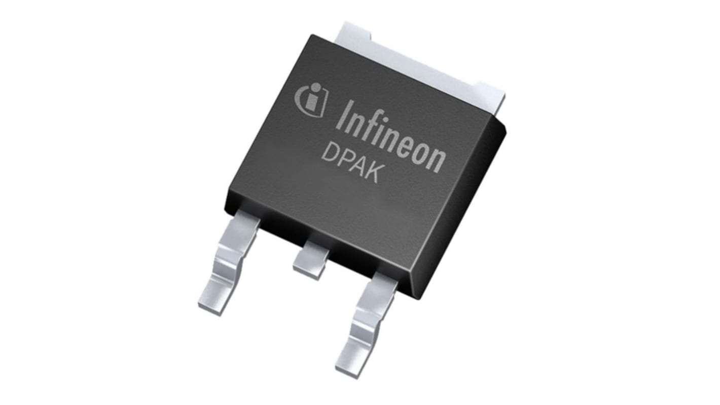
Infineon IPD068N10N3 G Type N-Channel MOSFET, 90 A, 100 V Enhancement, 5-Pin TO-252 IPD068N10N3GATMA1
- RS Stock No.:
- 171-1939
- Mfr. Part No.:
- IPD068N10N3GATMA1
- Brand:
- Infineon

Bulk discount available
View bulk pricing optionsSubtotal (1 pack of 10 units)*
£10.20
(exc. VAT)
£12.20
(inc. VAT)
FREE delivery for orders over £60.00
In Stock
- Plus 17,490 unit(s) shipping from 13 July 2026
Need more? Click ‘Check delivery dates’ to find extra stock and lead times.
Units | Per unit | Per Pack* |
|---|---|---|
| 10 - 90 | £1.02 | £10.20 |
| 100 - 240 | £0.822 | £8.22 |
| 250 - 490 | £0.782 | £7.82 |
| 500 - 990 | £0.718 | £7.18 |
| 1000 + | £0.631 | £6.31 |
*price indicative
- RS Stock No.:
- 171-1939
- Mfr. Part No.:
- IPD068N10N3GATMA1
- Brand:
- Infineon
Specifications
Technical Reference
Legislation and Compliance
Product Details
Find similar products by selecting one or more attributes.
Select all | Attribute | Value |
|---|---|---|
| Brand | Infineon | |
| Product Type | MOSFET | |
| Channel Type | Type N | |
| Maximum Continuous Drain Current Id | 90A | |
| Maximum Drain Source Voltage Vds | 100V | |
| Package Type | TO-252 | |
| Series | IPD068N10N3 G | |
| Mount Type | Surface | |
| Pin Count | 5 | |
| Maximum Drain Source Resistance Rds | 12.3mΩ | |
| Channel Mode | Enhancement | |
| Typical Gate Charge Qg @ Vgs | 51nC | |
| Maximum Power Dissipation Pd | 150W | |
| Forward Voltage Vf | 1V | |
| Minimum Operating Temperature | -55°C | |
| Maximum Operating Temperature | 175°C | |
| Height | 2.41mm | |
| Standards/Approvals | No | |
| Length | 6.73mm | |
| Automotive Standard | No | |
| Select all | ||
|---|---|---|
Brand Infineon | ||
Product Type MOSFET | ||
Channel Type Type N | ||
Maximum Continuous Drain Current Id 90A | ||
Maximum Drain Source Voltage Vds 100V | ||
Package Type TO-252 | ||
Series IPD068N10N3 G | ||
Mount Type Surface | ||
Pin Count 5 | ||
Maximum Drain Source Resistance Rds 12.3mΩ | ||
Channel Mode Enhancement | ||
Typical Gate Charge Qg @ Vgs 51nC | ||
Maximum Power Dissipation Pd 150W | ||
Forward Voltage Vf 1V | ||
Minimum Operating Temperature -55°C | ||
Maximum Operating Temperature 175°C | ||
Height 2.41mm | ||
Standards/Approvals No | ||
Length 6.73mm | ||
Automotive Standard No | ||
RoHS Status: Not Applicable
Infineon MOSFET
The Infineon PG-TO-252-3 surface mount N-channel MOSFET is a new age product with a drain-source resistance of 6.8mohm at a gate-source voltage of 10V. The MOSFET has continuous drain current of 90A. It has a maximum gate-source voltage of 20V and drain-source voltage of 100V. It has a maximum power dissipation of 71W. The MOSFET has a minimum and a maximum driving voltage of 6V and 10V respectively. It has been optimized for lower switching and conduction losses. The MOSFET offers excellent efficiency along with a long and productive life without compromising performance or functionality.
Features and Benefits
• Easy to design products
• Environmentally friendly
• Excellent gate charge x RDS (on) product (FOM)
• Excellent switching performance
• Halogen free
• Highest power density
• Increased efficiency
• Lead (Pb) free plating
• Less paralleling required
• Operating temperature ranges between -55°C and 175°C
• Smallest board space consumption
• Very low Qg and Qgd
• World's lowest RDS (on)
Applications
• Class D audio amplifiers
• Isolated DC-DC converters (telecom and data communication systems
• Motor control for 48V-80V systems (domestic vehicles, power tools, trucks)
• O-ring switches and circuit breakers in 48V systems
• Synchronous rectifier
Certifications
• ANSI/ESD S20.20:2014
• BS EN 61340-5-1:2007
• IEC61249-2-21
• JEDEC

Related links
- Infineon IPD068N10N3 G Type N-Channel MOSFET 100 V Enhancement, 5-Pin TO-252
- Infineon IPD053N08N3 G Type N-Channel MOSFET 80 V Enhancement, 5-Pin TO-252 IPD053N08N3GATMA1
- Infineon IPD053N08N3 G Type N-Channel MOSFET 80 V Enhancement, 5-Pin TO-252
- Infineon IPD25CN10N G Type N-Channel MOSFET 100 V Enhancement, 5-Pin TO-252 IPD25CN10NGATMA1
- Infineon IPD200N15N3 G Type N-Channel MOSFET 150 V Enhancement, 5-Pin TO-252 IPD200N15N3GATMA1
- Infineon IPD600N25N3 G Type N-Channel MOSFET 250 V Enhancement, 5-Pin TO-252
- Infineon IPD25CN10N G Type N-Channel MOSFET 100 V Enhancement, 5-Pin TO-252
- Infineon IPD200N15N3 G Type N-Channel MOSFET 150 V Enhancement, 5-Pin TO-252