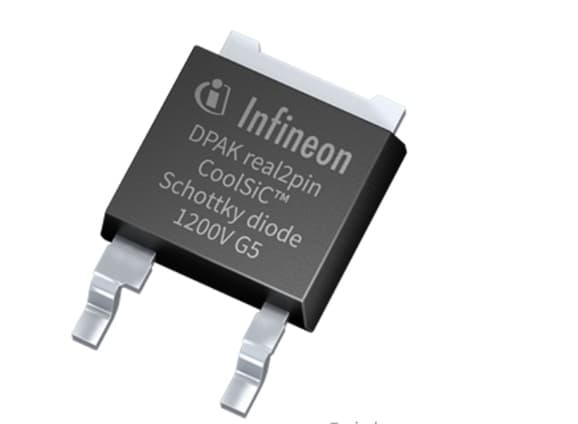
Infineon IPD053N08N3 G Type N-Channel MOSFET, 90 A, 80 V Enhancement, 5-Pin TO-252 IPD053N08N3GATMA1
- RS Stock No.:
- 171-1937
- Mfr. Part No.:
- IPD053N08N3GATMA1
- Brand:
- Infineon


Subtotal (1 pack of 10 units)*
£12.40
(exc. VAT)
£14.90
(inc. VAT)
FREE delivery for orders over £60.00
In Stock
- Plus 8,580 unit(s) shipping from 13 July 2026
Need more? Click ‘Check delivery dates’ to find extra stock and lead times.
Units | Per unit | Per Pack* |
|---|---|---|
| 10 + | £1.24 | £12.40 |
*price indicative
- RS Stock No.:
- 171-1937
- Mfr. Part No.:
- IPD053N08N3GATMA1
- Brand:
- Infineon
Specifications
Technical Reference
Legislation and Compliance
Product Details
Find similar products by selecting one or more attributes.
Select all | Attribute | Value |
|---|---|---|
| Brand | Infineon | |
| Channel Type | Type N | |
| Product Type | MOSFET | |
| Maximum Continuous Drain Current Id | 90A | |
| Maximum Drain Source Voltage Vds | 80V | |
| Package Type | TO-252 | |
| Series | IPD053N08N3 G | |
| Mount Type | Surface | |
| Pin Count | 5 | |
| Maximum Drain Source Resistance Rds | 9.5mΩ | |
| Channel Mode | Enhancement | |
| Maximum Power Dissipation Pd | 150W | |
| Typical Gate Charge Qg @ Vgs | 52nC | |
| Minimum Operating Temperature | -55°C | |
| Forward Voltage Vf | 1V | |
| Maximum Operating Temperature | 175°C | |
| Standards/Approvals | No | |
| Height | 2.41mm | |
| Length | 6.73mm | |
| Automotive Standard | No | |
| Select all | ||
|---|---|---|
Brand Infineon | ||
Channel Type Type N | ||
Product Type MOSFET | ||
Maximum Continuous Drain Current Id 90A | ||
Maximum Drain Source Voltage Vds 80V | ||
Package Type TO-252 | ||
Series IPD053N08N3 G | ||
Mount Type Surface | ||
Pin Count 5 | ||
Maximum Drain Source Resistance Rds 9.5mΩ | ||
Channel Mode Enhancement | ||
Maximum Power Dissipation Pd 150W | ||
Typical Gate Charge Qg @ Vgs 52nC | ||
Minimum Operating Temperature -55°C | ||
Forward Voltage Vf 1V | ||
Maximum Operating Temperature 175°C | ||
Standards/Approvals No | ||
Height 2.41mm | ||
Length 6.73mm | ||
Automotive Standard No | ||
RoHS Status: Not Applicable
Infineon MOSFET
The Infineon TO-252-3 surface mount N-channel MOSFET is a new age product with a drain-source resistance of 5.3mohm at a gate-source voltage of 10V. The MOSFET has continuous drain current of 90A. It has a maximum gate-source voltage of 20V and drain-source voltage of 80V. It has a maximum power dissipation of 150W. The MOSFET has a minimum and a maximum driving voltage of 6V and 10V respectively. It has been optimized for lower switching and conduction losses. The MOSFET tackles the most challenging applications giving full flexibility in limited spaces. It is designed to meet and exceed the energy efficiency and power density requirements of the sharpened next generation voltage regulation standards in computing applications. The MOSFET offers excellent efficiency along with a long and productive life without compromising performance or functionality.
Features and Benefits
• Dual sided cooling
• Excellent gate charge x RDS (ON) product (FOM)
• Lead (Pb) free plating
• Low parasitic inductance
• Low profile (<0, 7mm)
• Operating temperature ranges between -55°C and 175°C
• Optimized technology for DC-DC converters
• Superior thermal resistance
Applications
• AC-DC
• Adapter
• DC-DC
• LED
• Motor control
• PC power
• Server power supplies
• SMPS
• Solar
• Telecommunication
Certifications
• ANSI/ESD S20.20:2014
• BS EN 61340-5-1:2007
• IEC61249-2-21
• JEDEC

Related links
- Infineon IPD053N08N3 G Type N-Channel MOSFET 80 V Enhancement, 5-Pin TO-252
- Infineon IPD068N10N3 G Type N-Channel MOSFET 100 V Enhancement, 5-Pin TO-252 IPD068N10N3GATMA1
- Infineon IPD068N10N3 G Type N-Channel MOSFET 100 V Enhancement, 5-Pin TO-252
- Infineon IPD25CN10N G Type N-Channel MOSFET 100 V Enhancement, 5-Pin TO-252 IPD25CN10NGATMA1
- Infineon IPD200N15N3 G Type N-Channel MOSFET 150 V Enhancement, 5-Pin TO-252 IPD200N15N3GATMA1
- Infineon IPD600N25N3 G Type N-Channel MOSFET 250 V Enhancement, 5-Pin TO-252
- Infineon IPD25CN10N G Type N-Channel MOSFET 100 V Enhancement, 5-Pin TO-252
- Infineon IPD200N15N3 G Type N-Channel MOSFET 150 V Enhancement, 5-Pin TO-252