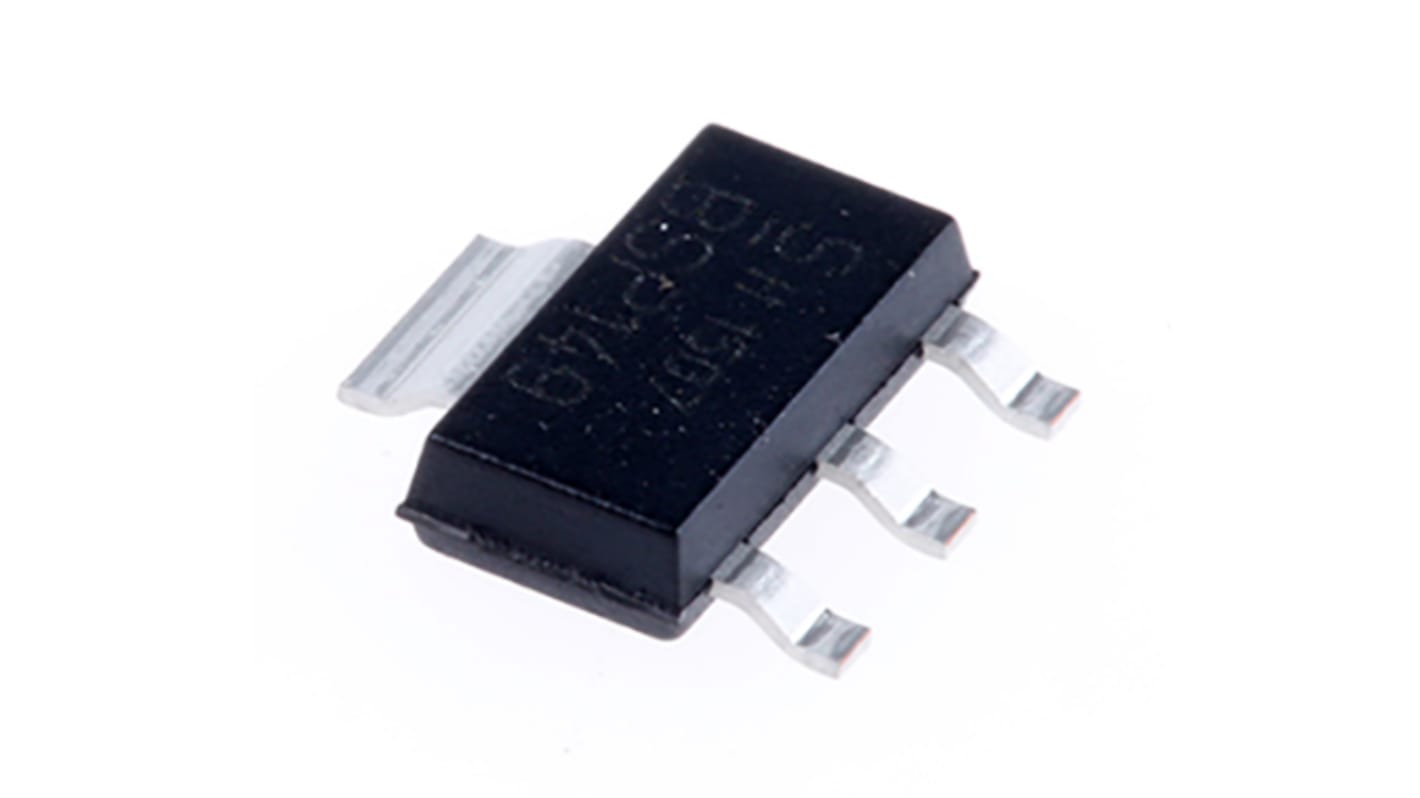
Infineon SIPMOS Type N-Channel MOSFET, 660 mA, 200 V Depletion, 4-Pin SOT-223
- RS Stock No.:
- 911-4808
- Mfr. Part No.:
- BSP149H6327XTSA1
- Brand:
- Infineon

Subtotal (1 reel of 1000 units)*
£319.00
(exc. VAT)
£383.00
(inc. VAT)
FREE delivery for orders over £60.00
Temporarily out of stock
- Shipping from 07 December 2026
Need more? Click ‘Check delivery dates’ to find extra stock and lead times.
Units | Per unit | Per Reel* |
|---|---|---|
| 1000 + | £0.319 | £319.00 |
*price indicative
- RS Stock No.:
- 911-4808
- Mfr. Part No.:
- BSP149H6327XTSA1
- Brand:
- Infineon
Specifications
Technical Reference
Legislation and Compliance
Product Details
Find similar products by selecting one or more attributes.
Select all | Attribute | Value |
|---|---|---|
| Brand | Infineon | |
| Channel Type | Type N | |
| Product Type | MOSFET | |
| Maximum Continuous Drain Current Id | 660mA | |
| Maximum Drain Source Voltage Vds | 200V | |
| Series | SIPMOS | |
| Package Type | SOT-223 | |
| Mount Type | Surface | |
| Pin Count | 4 | |
| Maximum Drain Source Resistance Rds | 1.8Ω | |
| Channel Mode | Depletion | |
| Maximum Power Dissipation Pd | 1.8W | |
| Typical Gate Charge Qg @ Vgs | 11nC | |
| Forward Voltage Vf | 1.2V | |
| Minimum Operating Temperature | -55°C | |
| Maximum Operating Temperature | 150°C | |
| Height | 1.6mm | |
| Standards/Approvals | No | |
| Length | 6.5mm | |
| Automotive Standard | AEC-Q101 | |
| Select all | ||
|---|---|---|
Brand Infineon | ||
Channel Type Type N | ||
Product Type MOSFET | ||
Maximum Continuous Drain Current Id 660mA | ||
Maximum Drain Source Voltage Vds 200V | ||
Series SIPMOS | ||
Package Type SOT-223 | ||
Mount Type Surface | ||
Pin Count 4 | ||
Maximum Drain Source Resistance Rds 1.8Ω | ||
Channel Mode Depletion | ||
Maximum Power Dissipation Pd 1.8W | ||
Typical Gate Charge Qg @ Vgs 11nC | ||
Forward Voltage Vf 1.2V | ||
Minimum Operating Temperature -55°C | ||
Maximum Operating Temperature 150°C | ||
Height 1.6mm | ||
Standards/Approvals No | ||
Length 6.5mm | ||
Automotive Standard AEC-Q101 | ||
- COO (Country of Origin):
- MY
Infineon SIPMOS® Series MOSFET, 660mA Maximum Continuous Drain Current, 1.8W Maximum Power Dissipation - BSP149H6327XTSA1
This MOSFET is an essential component designed for a range of electronic applications, offering efficient performance within a compact surface mount package. It is well-suited for controlling automation circuits and is relevant for users in the electronics, electrical, and mechanical sectors. The depletion mode characteristic enhances control for switching applications, making it a suitable choice for engineers.
Features & Benefits
• Maximum drain-source voltage of 200V for high voltage applications
• Continuous drain current capability of up to 660mA
• Utilises SIPMOS technology for consistent performance
• RoHS compliant with Pb-free lead plating
• dv/dt rated for improved resilience against voltage variations
Applications
• Driver in automation systems
• Switching power supplies for energy management
• Automotive electronics compliant with AEC-Q101 standards
What is the significance of the depletion mode characteristic?
The depletion mode allows for efficient control of the MOSFET, which enables effective switching even at lower voltages, beneficial in diverse electronic designs.
How does the device manage thermal challenges?
It functions within a broad temperature range of -55°C to +150°C, ensuring dependable performance even under extreme thermal conditions, supported by its effective thermal management capabilities.
What are the gate threshold voltage values for this component?
The gate threshold voltage ranges from -2.1V to -1V, providing versatile switching options for different circuit requirements.
What are the implications of the ESD Class rating?
The ESD Class rating of 1B indicates a design that can withstand electrostatic discharge levels between 500V and 600V, enhancing the device's reliability in sensitive applications.

Related links
- Infineon SIPMOS Type N-Channel MOSFET 200 V Depletion, 4-Pin SOT-223 BSP149H6327XTSA1
- Infineon SIPMOS Type N-Channel MOSFET 200 V Enhancement, 4-Pin SOT-223
- Infineon SIPMOS Type N-Channel MOSFET 200 V Enhancement, 4-Pin SOT-223 BSP297H6327XTSA1
- Infineon SIPMOS Type N-Channel MOSFET 600 V Depletion, 4-Pin SOT-223
- Infineon SIPMOS Type N-Channel MOSFET 600 V Depletion, 4-Pin SOT-223 BSP135H6327XTSA1
- Infineon SIPMOS Type N-Channel MOSFET 240 V Depletion, 4-Pin SOT-223 BSP129H6327XTSA1
- Infineon SIPMOS Type N-Channel MOSFET 600 V Depletion, 3-Pin SOT-23
- Infineon SIPMOS Type N-Channel MOSFET 60 V Depletion, 3-Pin SOT-23 BSS159NH6327XTSA2