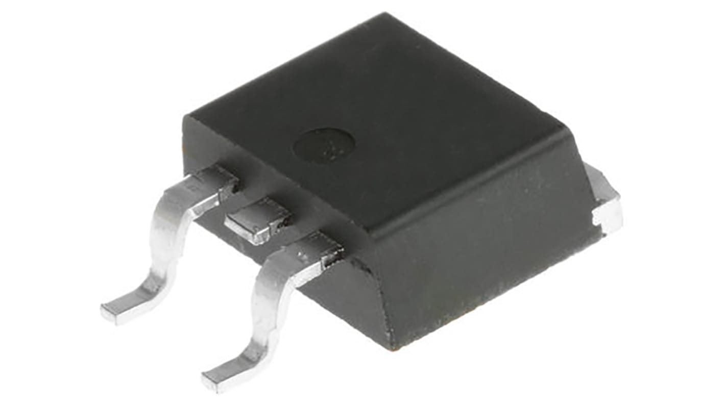
onsemi QFET Type P-Channel MOSFET, 11.5 A, 200 V Enhancement, 3-Pin TO-263
- RS Stock No.:
- 166-2528
- Mfr. Part No.:
- FQB12P20TM
- Brand:
- onsemi

Subtotal (1 reel of 800 units)*
£582.40
(exc. VAT)
£699.20
(inc. VAT)
FREE delivery for orders over £60.00
Temporarily out of stock
- Shipping from 12 October 2026
Need more? Click ‘Check delivery dates’ to find extra stock and lead times.
Units | Per unit | Per Reel* |
|---|---|---|
| 800 + | £0.728 | £582.40 |
*price indicative
- RS Stock No.:
- 166-2528
- Mfr. Part No.:
- FQB12P20TM
- Brand:
- onsemi
Specifications
Technical Reference
Legislation and Compliance
Product Details
Find similar products by selecting one or more attributes.
Select all | Attribute | Value |
|---|---|---|
| Brand | onsemi | |
| Channel Type | Type P | |
| Product Type | MOSFET | |
| Maximum Continuous Drain Current Id | 11.5A | |
| Maximum Drain Source Voltage Vds | 200V | |
| Series | QFET | |
| Package Type | TO-263 | |
| Mount Type | Surface | |
| Pin Count | 3 | |
| Maximum Drain Source Resistance Rds | 470mΩ | |
| Channel Mode | Enhancement | |
| Forward Voltage Vf | -5V | |
| Minimum Operating Temperature | -55°C | |
| Typical Gate Charge Qg @ Vgs | 31nC | |
| Maximum Power Dissipation Pd | 3.13W | |
| Maximum Operating Temperature | 150°C | |
| Height | 4.83mm | |
| Standards/Approvals | No | |
| Length | 10.67mm | |
| Automotive Standard | No | |
| Select all | ||
|---|---|---|
Brand onsemi | ||
Channel Type Type P | ||
Product Type MOSFET | ||
Maximum Continuous Drain Current Id 11.5A | ||
Maximum Drain Source Voltage Vds 200V | ||
Series QFET | ||
Package Type TO-263 | ||
Mount Type Surface | ||
Pin Count 3 | ||
Maximum Drain Source Resistance Rds 470mΩ | ||
Channel Mode Enhancement | ||
Forward Voltage Vf -5V | ||
Minimum Operating Temperature -55°C | ||
Typical Gate Charge Qg @ Vgs 31nC | ||
Maximum Power Dissipation Pd 3.13W | ||
Maximum Operating Temperature 150°C | ||
Height 4.83mm | ||
Standards/Approvals No | ||
Length 10.67mm | ||
Automotive Standard No | ||
Enhancement Mode P-Channel MOSFET, ON Semiconductor
ON Semiconductors range of P-Channel MOSFETS are produced using ON Semi’s proprietary, high cell density, DMOS technology. This very high density process has been designed to minimize on-state resistance to provide a rugged and reliable performance for fast switching.
Features and Benefits:
• Voltage controlled P-Channel small signal switch
• High-Density cell design
• High saturation current
• Superior switching
• Great rugged and reliable performance
• DMOS technology
Applications:
• Load Switching
• DC/DC converter
• Battery protection
• Power management control
• DC motor control
MOSFET Transistors, ON Semi
ON Semi offers a substantial portfolio of MOSFET devices that includes high-voltage (>250V) and low-voltage (<250V) types. The Advanced silicon technology provides smaller die sizes, which it is incorporated into multiple industry-standard and thermally-enhanced packages.
ON Semi MOSFETs provide superior design reliability from reduced voltage spikes and overshoot, to lower junction capacitance and reverse recovery charge, to elimination of additional external components to keep systems up and running longer.
Related links
- onsemi QFET Type P-Channel MOSFET 200 V Enhancement, 3-Pin TO-263 FQB12P20TM
- onsemi QFET Type P-Channel MOSFET 100 V Enhancement, 3-Pin TO-263
- onsemi QFET Type P-Channel MOSFET 100 V Enhancement, 3-Pin TO-263
- onsemi QFET Type P-Channel MOSFET 60 V Enhancement, 3-Pin TO-263
- onsemi QFET Type P-Channel MOSFET 100 V Enhancement, 3-Pin TO-263 FQB22P10TM
- onsemi QFET Type P-Channel MOSFET 100 V Enhancement, 3-Pin TO-263 FQB34P10TM
- onsemi QFET Type P-Channel MOSFET 60 V Enhancement, 3-Pin TO-263 FQB27P06TM
- onsemi QFET Type P-Channel MOSFET 60 V Enhancement, 3-Pin TO-263 FQB47P06TM-AM002