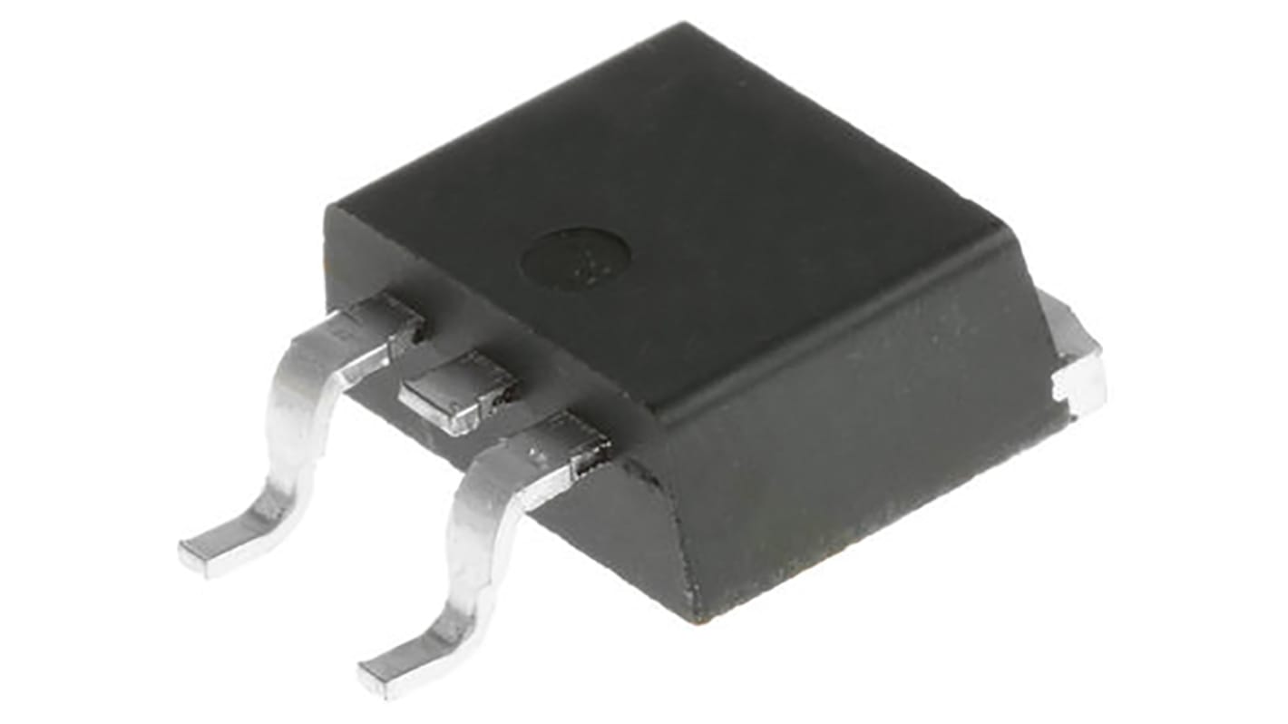
Infineon HEXFET Type N-Channel MOSFET, 33 A, 100 V Enhancement, 3-Pin TO-263
- RS Stock No.:
- 165-5894
- Mfr. Part No.:
- IRF540NSTRLPBF
- Brand:
- Infineon

Subtotal (1 reel of 800 units)*
£425.60
(exc. VAT)
£510.40
(inc. VAT)
FREE delivery for orders over £60.00
In Stock
- 31,200 unit(s) ready to ship
Need more? Click ‘Check delivery dates’ to find extra stock and lead times.
Units | Per unit | Per Reel* |
|---|---|---|
| 800 + | £0.532 | £425.60 |
*price indicative
- RS Stock No.:
- 165-5894
- Mfr. Part No.:
- IRF540NSTRLPBF
- Brand:
- Infineon
Specifications
Technical Reference
Legislation and Compliance
Product Details
Find similar products by selecting one or more attributes.
Select all | Attribute | Value |
|---|---|---|
| Brand | Infineon | |
| Channel Type | Type N | |
| Product Type | MOSFET | |
| Maximum Continuous Drain Current Id | 33A | |
| Maximum Drain Source Voltage Vds | 100V | |
| Package Type | TO-263 | |
| Series | HEXFET | |
| Mount Type | Surface | |
| Pin Count | 3 | |
| Maximum Drain Source Resistance Rds | 44mΩ | |
| Channel Mode | Enhancement | |
| Forward Voltage Vf | 1.2V | |
| Minimum Operating Temperature | -55°C | |
| Maximum Power Dissipation Pd | 130W | |
| Typical Gate Charge Qg @ Vgs | 71nC | |
| Maximum Operating Temperature | 175°C | |
| Height | 4.83mm | |
| Length | 10.67mm | |
| Standards/Approvals | No | |
| Automotive Standard | No | |
| Select all | ||
|---|---|---|
Brand Infineon | ||
Channel Type Type N | ||
Product Type MOSFET | ||
Maximum Continuous Drain Current Id 33A | ||
Maximum Drain Source Voltage Vds 100V | ||
Package Type TO-263 | ||
Series HEXFET | ||
Mount Type Surface | ||
Pin Count 3 | ||
Maximum Drain Source Resistance Rds 44mΩ | ||
Channel Mode Enhancement | ||
Forward Voltage Vf 1.2V | ||
Minimum Operating Temperature -55°C | ||
Maximum Power Dissipation Pd 130W | ||
Typical Gate Charge Qg @ Vgs 71nC | ||
Maximum Operating Temperature 175°C | ||
Height 4.83mm | ||
Length 10.67mm | ||
Standards/Approvals No | ||
Automotive Standard No | ||
- COO (Country of Origin):
- MX
Infineon HEXFET Series MOSFET, 33A Maximum Continuous Drain Current, 130W Maximum Power Dissipation - IRF540NSTRLPBF
This high power MOSFET is designed for efficiency and reliability across a variety of applications. Featuring an N-channel configuration, it operates in enhancement mode with a maximum continuous drain current of 33A and a breakdown voltage of 100V. Its surface mount design allows for simple integration into printed circuit boards, enhancing versatility in modern applications.
Features & Benefits
• Low Rds(on) of 44mΩ improves circuit efficiency
• High power dissipation capability of 130W supports robust applications
• Fast switching speed minimises energy loss during operation
• Wide operating temperature range from -55°C to +175°C suits diverse environments
• Lead-free construction adheres to contemporary environmental standards
Applications
• Power management in automation systems
• High-efficiency power supplies for electronics
• Motor control in electrical engineering
• Renewable energy systems for effective energy conversion
What is the maximum gate-to-source voltage for this device?
The maximum gate-to-source voltage is ±20V, allowing for safe operation in typical circuits.
How does this device handle thermal management?
With a maximum power dissipation of 130W and a junction-to-case thermal resistance of 1.15°C/W, it effectively manages heat during operation.
What is the typical gate charge at 10V?
The typical gate charge at a gate-to-source voltage of 10V is 71 nC, ensuring quick response times in switching applications.
Can this device be mounted on standard PCBs?
Yes, it is designed in a D2PAK package, making it suitable for surface mount applications on standard PCB layouts.
What is the significance of the enhancement mode in this MOSFET?
The enhancement mode allows for greater control over the conduction state, providing improved performance in switching applications.

Related links
- Infineon HEXFET Type N-Channel MOSFET 100 V Enhancement, 3-Pin TO-263 IRF540NSTRLPBF
- Infineon HEXFET Type N-Channel MOSFET 100 V Enhancement, 3-Pin TO-263 IRF540NSTRRPBF
- Infineon HEXFET Type N-Channel MOSFET 150 V Enhancement, 3-Pin TO-263
- Infineon HEXFET Type N-Channel MOSFET 150 V Enhancement, 3-Pin TO-263 IRFS4615TRLPBF
- Infineon HEXFET Type N-Channel MOSFET 100 V Enhancement, 3-Pin TO-247
- Infineon HEXFET Type N-Channel MOSFET 100 V Enhancement, 3-Pin TO-262
- Infineon HEXFET Type N-Channel MOSFET 100 V Enhancement, 3-Pin TO-220 IRF540NPBF
- Infineon HEXFET Type N-Channel MOSFET 100 V Enhancement, 3-Pin TO-247 IRFP140NPBF