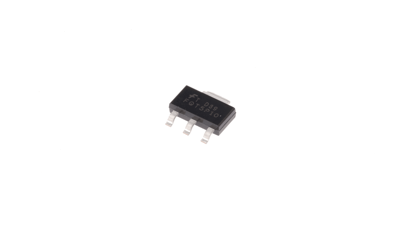
onsemi QFET Type P-Channel MOSFET, 1 A, 100 V Enhancement, 4-Pin SOT-223
- RS Stock No.:
- 124-1723
- Mfr. Part No.:
- FQT5P10TF
- Brand:
- onsemi

Subtotal (1 reel of 4000 units)*
£648.00
(exc. VAT)
£776.00
(inc. VAT)
FREE delivery for orders over £60.00
Last RS stock
- Final 12,000 unit(s), ready to ship
Units | Per unit | Per Reel* |
|---|---|---|
| 4000 + | £0.162 | £648.00 |
*price indicative
- RS Stock No.:
- 124-1723
- Mfr. Part No.:
- FQT5P10TF
- Brand:
- onsemi
Specifications
Technical Reference
Legislation and Compliance
Product Details
Find similar products by selecting one or more attributes.
Select all | Attribute | Value |
|---|---|---|
| Brand | onsemi | |
| Product Type | MOSFET | |
| Channel Type | Type P | |
| Maximum Continuous Drain Current Id | 1A | |
| Maximum Drain Source Voltage Vds | 100V | |
| Series | QFET | |
| Package Type | SOT-223 | |
| Mount Type | Surface | |
| Pin Count | 4 | |
| Maximum Drain Source Resistance Rds | 1.05Ω | |
| Channel Mode | Enhancement | |
| Typical Gate Charge Qg @ Vgs | 6.3nC | |
| Maximum Power Dissipation Pd | 2W | |
| Forward Voltage Vf | -4V | |
| Minimum Operating Temperature | -55°C | |
| Maximum Operating Temperature | 150°C | |
| Standards/Approvals | No | |
| Length | 6.5mm | |
| Height | 1.6mm | |
| Automotive Standard | No | |
| Select all | ||
|---|---|---|
Brand onsemi | ||
Product Type MOSFET | ||
Channel Type Type P | ||
Maximum Continuous Drain Current Id 1A | ||
Maximum Drain Source Voltage Vds 100V | ||
Series QFET | ||
Package Type SOT-223 | ||
Mount Type Surface | ||
Pin Count 4 | ||
Maximum Drain Source Resistance Rds 1.05Ω | ||
Channel Mode Enhancement | ||
Typical Gate Charge Qg @ Vgs 6.3nC | ||
Maximum Power Dissipation Pd 2W | ||
Forward Voltage Vf -4V | ||
Minimum Operating Temperature -55°C | ||
Maximum Operating Temperature 150°C | ||
Standards/Approvals No | ||
Length 6.5mm | ||
Height 1.6mm | ||
Automotive Standard No | ||
QFET® P-Channel MOSFET, Fairchild Semiconductor
Fairchild Semiconductor’s new QFET® Planar MOSFETs use advanced, proprietary technology to offer best-in-class operating performance for a wide range of applications, including power supplies, PFC (Power Factor Correction), DC-DC Converters, Plasma Display Panels (PDP), lighting ballasts, and motion control.
They offer reduced on-state loss by lowering on-resistance (RDS(on)), and reduced switching loss by lowering gate charge (Qg) and output capacitance (Coss). By using Advanced QFET® process technology, Fairchild can offer an improved figure of merit (FOM) over competing Planar MOSFET devices.
MOSFET Transistors, ON Semi
ON Semi offers a substantial portfolio of MOSFET devices that includes high-voltage (>250V) and low-voltage (<250V) types. The Advanced silicon technology provides smaller die sizes, which it is incorporated into multiple industry-standard and thermally-enhanced packages.
ON Semi MOSFETs provide superior design reliability from reduced voltage spikes and overshoot, to lower junction capacitance and reverse recovery charge, to elimination of additional external components to keep systems up and running longer.
Related links
- onsemi QFET Type P-Channel MOSFET 100 V Enhancement, 4-Pin SOT-223 FQT5P10TF
- onsemi QFET Type N-Channel MOSFET 100 V Enhancement, 4-Pin SOT-223
- onsemi QFET Type N-Channel MOSFET 200 V Enhancement, 4-Pin SOT-223
- onsemi QFET Type N-Channel MOSFET 100 V Enhancement, 4-Pin SOT-223 FQT7N10LTF
- onsemi QFET Type N-Channel MOSFET 200 V Enhancement, 4-Pin SOT-223 FQT4N20LTF
- Infineon SIPMOS Type P-Channel MOSFET 100 V Enhancement, 4-Pin SOT-223 BSP322PH6327XTSA1
- Infineon SIPMOS Type P-Channel MOSFET 100 V Enhancement, 4-Pin SOT-223
- onsemi QFET Type P-Channel MOSFET 60 V Enhancement, 3-Pin TO-252