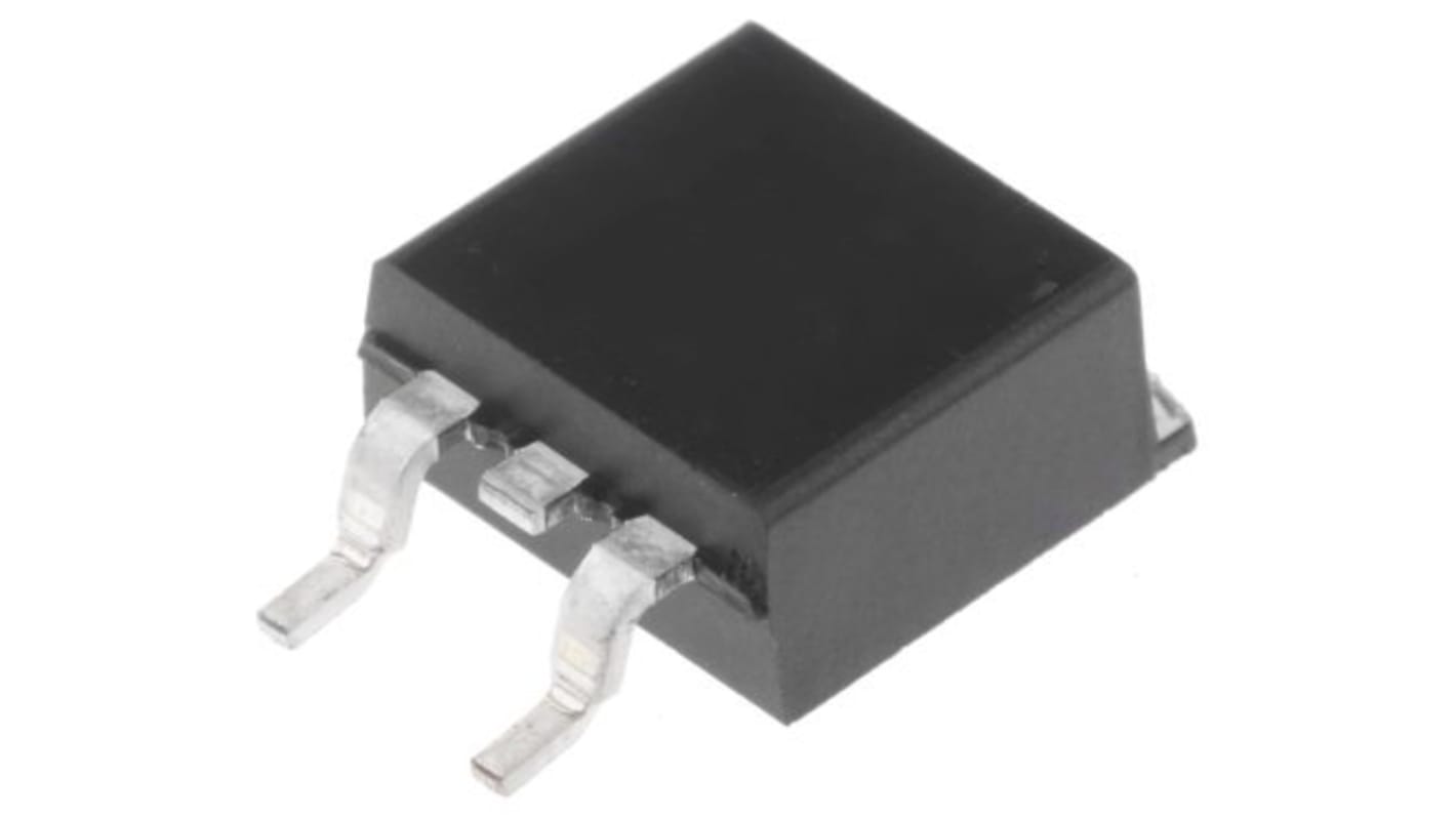
onsemi Type N-Channel MOSFET, 36 A, 650 V Enhancement, 3-Pin TO-263
- RS Stock No.:
- 189-0252
- Mfr. Part No.:
- NTB095N65S3HF
- Brand:
- onsemi

Subtotal (1 reel of 800 units)*
£2,514.40
(exc. VAT)
£3,017.60
(inc. VAT)
FREE delivery for orders over £60.00
Temporarily out of stock
- Shipping from 09 November 2026
Need more? Click ‘Check delivery dates’ to find extra stock and lead times.
Units | Per unit | Per Reel* |
|---|---|---|
| 800 + | £3.143 | £2,514.40 |
*price indicative
- RS Stock No.:
- 189-0252
- Mfr. Part No.:
- NTB095N65S3HF
- Brand:
- onsemi
Specifications
Technical Reference
Legislation and Compliance
Product Details
Find similar products by selecting one or more attributes.
Select all | Attribute | Value |
|---|---|---|
| Brand | onsemi | |
| Channel Type | Type N | |
| Product Type | MOSFET | |
| Maximum Continuous Drain Current Id | 36A | |
| Maximum Drain Source Voltage Vds | 650V | |
| Package Type | TO-263 | |
| Mount Type | Surface | |
| Pin Count | 3 | |
| Maximum Drain Source Resistance Rds | 95mΩ | |
| Channel Mode | Enhancement | |
| Typical Gate Charge Qg @ Vgs | 66nC | |
| Minimum Operating Temperature | -55°C | |
| Maximum Power Dissipation Pd | 272W | |
| Forward Voltage Vf | 1.3V | |
| Maximum Operating Temperature | 150°C | |
| Length | 10.67mm | |
| Standards/Approvals | No | |
| Height | 4.58mm | |
| Automotive Standard | No | |
| Select all | ||
|---|---|---|
Brand onsemi | ||
Channel Type Type N | ||
Product Type MOSFET | ||
Maximum Continuous Drain Current Id 36A | ||
Maximum Drain Source Voltage Vds 650V | ||
Package Type TO-263 | ||
Mount Type Surface | ||
Pin Count 3 | ||
Maximum Drain Source Resistance Rds 95mΩ | ||
Channel Mode Enhancement | ||
Typical Gate Charge Qg @ Vgs 66nC | ||
Minimum Operating Temperature -55°C | ||
Maximum Power Dissipation Pd 272W | ||
Forward Voltage Vf 1.3V | ||
Maximum Operating Temperature 150°C | ||
Length 10.67mm | ||
Standards/Approvals No | ||
Height 4.58mm | ||
Automotive Standard No | ||
SUPERFET III MOSFET is ON Semiconductor’s brand-new high voltage super-junction (SJ) MOSFET family that is utilizing charge balance technology for outstanding low on-resistance and lower gate charge performance. This advanced technology is tailored to minimize conduction loss, provide superior switching performance, and withstand extreme dv/dt rate. Consequently, SUPERFET III MOSFET is very suitable for the various power systems for miniaturization and higher efficiency. SUPERFET III FRFET MOSFET’s optimized reverse recovery performance of body diode can remove additional component and improve system reliability.
700 V @ TJ = 150 °C
Ultra Low Gate Charge (Typ. Qg = 66 nC)
Low Effective Output Capacitance (Typ. Coss(eff.) = 569 pF)
Excellent body diode performance (low Qrr, robust body diode)
Optimized Capacitance
Typ. RDS(on) = 80 mΩHigher system reliability at low temperature operation
Lower switching loss
Higher system reliability in LLC and Phase shift full bridge circuit
Lower peak Vds and lower Vgs oscillation
Applications
Telecommunication
Cloud system
Industrial
End Products
Telecom power
Server power
EV charger
Solar / UPS
Related links
- onsemi Type N-Channel MOSFET 650 V Enhancement, 3-Pin TO-263 NTB095N65S3HF
- onsemi Type N-Channel MOSFET 650 V Enhancement, 3-Pin TO-220
- onsemi Type N-Channel MOSFET 650 V Enhancement, 3-Pin TO-220 NTP095N65S3HF
- onsemi Type N-Channel MOSFET 650 V Enhancement, 3-Pin TO-263
- onsemi Type N-Channel MOSFET 650 V Enhancement, 3-Pin TO-263
- onsemi Type N-Channel MOSFET 650 V Enhancement, 3-Pin TO-263
- onsemi Type N-Channel MOSFET 650 V Enhancement, 3-Pin TO-263
- onsemi Type N-Channel MOSFET 650 V Enhancement, 3-Pin TO-263 NVB082N65S3F