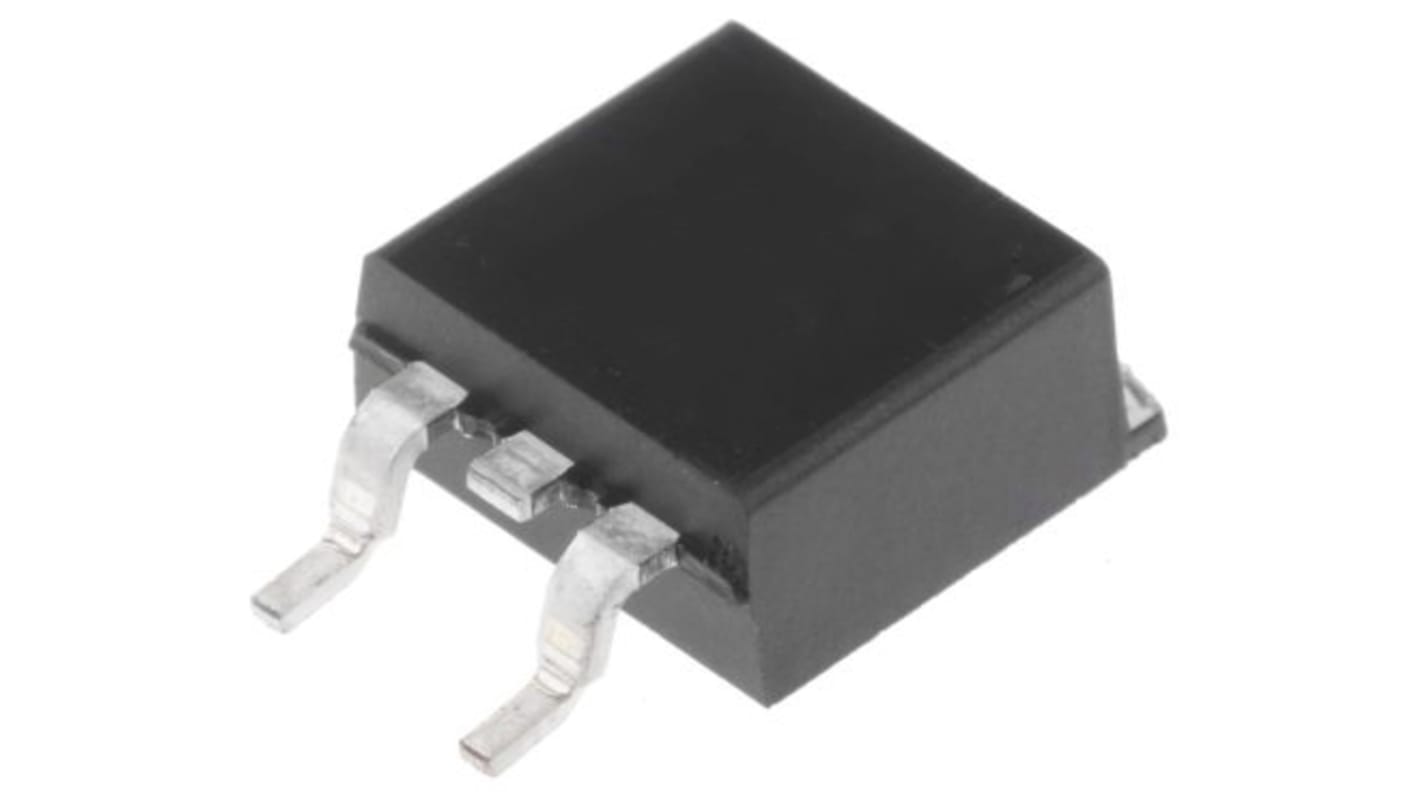
onsemi SuperFET III MOSFET Easy-drive Type N-Channel MOSFET, 44 A, 650 V Enhancement, 3-Pin TO-263 NVB072N65S3
- RS Stock No.:
- 186-1461
- Mfr. Part No.:
- NVB072N65S3
- Brand:
- onsemi

Currently unavailable
We don't know if this item will be back in stock, RS intend to remove it from our range soon.
- RS Stock No.:
- 186-1461
- Mfr. Part No.:
- NVB072N65S3
- Brand:
- onsemi
Specifications
Technical Reference
Legislation and Compliance
Product Details
Find similar products by selecting one or more attributes.
Select all | Attribute | Value |
|---|---|---|
| Brand | onsemi | |
| Channel Type | Type N | |
| Product Type | MOSFET | |
| Maximum Continuous Drain Current Id | 44A | |
| Maximum Drain Source Voltage Vds | 650V | |
| Package Type | TO-263 | |
| Series | SuperFET III MOSFET Easy-drive | |
| Mount Type | Surface | |
| Pin Count | 3 | |
| Maximum Drain Source Resistance Rds | 107mΩ | |
| Channel Mode | Enhancement | |
| Typical Gate Charge Qg @ Vgs | 82nC | |
| Maximum Power Dissipation Pd | 312W | |
| Minimum Operating Temperature | -55°C | |
| Maximum Operating Temperature | 150°C | |
| Height | 4.58mm | |
| Standards/Approvals | No | |
| Length | 10.67mm | |
| Automotive Standard | AEC-Q101 | |
| Select all | ||
|---|---|---|
Brand onsemi | ||
Channel Type Type N | ||
Product Type MOSFET | ||
Maximum Continuous Drain Current Id 44A | ||
Maximum Drain Source Voltage Vds 650V | ||
Package Type TO-263 | ||
Series SuperFET III MOSFET Easy-drive | ||
Mount Type Surface | ||
Pin Count 3 | ||
Maximum Drain Source Resistance Rds 107mΩ | ||
Channel Mode Enhancement | ||
Typical Gate Charge Qg @ Vgs 82nC | ||
Maximum Power Dissipation Pd 312W | ||
Minimum Operating Temperature -55°C | ||
Maximum Operating Temperature 150°C | ||
Height 4.58mm | ||
Standards/Approvals No | ||
Length 10.67mm | ||
Automotive Standard AEC-Q101 | ||
Non Compliant
SUPERFET III MOSFET is ON Semiconductor’s brand−new high voltage super−junction (SJ) MOSFET family that is utilizing charge balance technology for outstanding low on−resistance and lower gate charge performance. This advanced technology is tailored to minimize conduction loss, provide superior switching performance, and withstand extreme dv/dt rate. Consequently, SUPERFET III MOSFET Easy drive series helps manage EMI issues and allows for easier design implementation.
700 V @ TJ = 150°C
Ultra Low Gate Charge (Typ. Qg = 78 nC)
Low Effective Output Capacitance (Typ. Coss(eff.) = 715 pF)
PPAP Capable
Typ. RDS(on) = 63 mΩ
Higher system reliability at low temperature operation
Lower switching loss
PPAP Capable
Applications
HV DC/DC converter
End Products
On Board Charger
DC/DC Converter
Related links
- onsemi SuperFET III MOSFET Easy-drive Type N-Channel MOSFET 650 V Enhancement, 3-Pin TO-263
- onsemi SuperFET III MOSFET Easy-drive Type N-Channel MOSFET 650 V Enhancement, 3-Pin TO-247 NVHL072N65S3
- onsemi SUPERFET III Type N-Channel Power MOSFET 650 V Enhancement, 3-Pin TO-220
- onsemi SUPERFET III Type N-Channel Power MOSFET 650 V Enhancement, 3-Pin TO-220 FCP165N65S3
- onsemi SUPERFET III Type N-Channel MOSFET & Diode 650 V Enhancement, 3-Pin TO-263
- onsemi SUPERFET III Type N-Channel MOSFET & Diode 650 V Enhancement, 3-Pin TO-263 FCB125N65S3
- onsemi SUPERFET III Type N-Channel MOSFET 650 V N, 3-Pin TO-220
- onsemi SUPERFET III Type N-Channel MOSFET 650 V N, 3-Pin TO-220