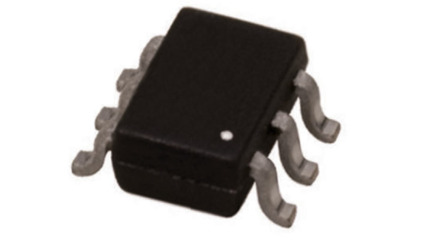
onsemi Isolated PowerTrench 2 Type N-Channel MOSFET, 2.5 A, 30 V Enhancement, 6-Pin SOT-23
- RS Stock No.:
- 166-2973
- Mfr. Part No.:
- FDC6561AN
- Brand:
- onsemi

Subtotal (1 reel of 3000 units)*
£423.00
(exc. VAT)
£507.00
(inc. VAT)
FREE delivery for orders over £60.00
- 27,000 unit(s) ready to ship
Units | Per unit | Per Reel* |
|---|---|---|
| 3000 + | £0.141 | £423.00 |
*price indicative
- RS Stock No.:
- 166-2973
- Mfr. Part No.:
- FDC6561AN
- Brand:
- onsemi
Select all | Attribute | Value |
|---|---|---|
| Brand | onsemi | |
| Channel Type | Type N | |
| Product Type | MOSFET | |
| Maximum Continuous Drain Current Id | 2.5A | |
| Maximum Drain Source Voltage Vds | 30V | |
| Package Type | SOT-23 | |
| Series | PowerTrench | |
| Mount Type | Surface | |
| Pin Count | 6 | |
| Maximum Drain Source Resistance Rds | 152mΩ | |
| Channel Mode | Enhancement | |
| Minimum Operating Temperature | -55°C | |
| Typical Gate Charge Qg @ Vgs | 2.3nC | |
| Maximum Power Dissipation Pd | 960mW | |
| Forward Voltage Vf | 0.78V | |
| Transistor Configuration | Isolated | |
| Maximum Operating Temperature | 150°C | |
| Standards/Approvals | No | |
| Length | 3mm | |
| Height | 1mm | |
| Number of Elements per Chip | 2 | |
| Automotive Standard | No | |
| Select all | ||
|---|---|---|
Brand onsemi | ||
Channel Type Type N | ||
Product Type MOSFET | ||
Maximum Continuous Drain Current Id 2.5A | ||
Maximum Drain Source Voltage Vds 30V | ||
Package Type SOT-23 | ||
Series PowerTrench | ||
Mount Type Surface | ||
Pin Count 6 | ||
Maximum Drain Source Resistance Rds 152mΩ | ||
Channel Mode Enhancement | ||
Minimum Operating Temperature -55°C | ||
Typical Gate Charge Qg @ Vgs 2.3nC | ||
Maximum Power Dissipation Pd 960mW | ||
Forward Voltage Vf 0.78V | ||
Transistor Configuration Isolated | ||
Maximum Operating Temperature 150°C | ||
Standards/Approvals No | ||
Length 3mm | ||
Height 1mm | ||
Number of Elements per Chip 2 | ||
Automotive Standard No | ||
PowerTrench® Dual N-Channel MOSFET, Fairchild Semiconductor
MOSFET Transistors, ON Semi
Related links
- onsemi Isolated PowerTrench 2 Type N-Channel MOSFET 30 V Enhancement, 6-Pin SOT-23 FDC6561AN
- onsemi Isolated PowerTrench 2 Type P 2.5 A 6-Pin SOT-23
- onsemi Isolated PowerTrench 2 Type P 2.5 A 6-Pin SOT-23 FDC6333C
- onsemi Isolated PowerTrench 2 Type N-Channel MOSFET 20 V Enhancement, 6-Pin SOT-23
- onsemi Isolated PowerTrench 2 Type P 2.7 A 6-Pin SOT-23
- onsemi Isolated PowerTrench 2 Type N-Channel MOSFET 20 V Enhancement, 6-Pin SOT-23 FDC6305N
- onsemi Isolated PowerTrench 2 Type N-Channel MOSFET 20 V Enhancement, 6-Pin SOT-23
- onsemi Isolated PowerTrench 2 Type P 2.7 A 6-Pin SOT-23 FDC6327C
