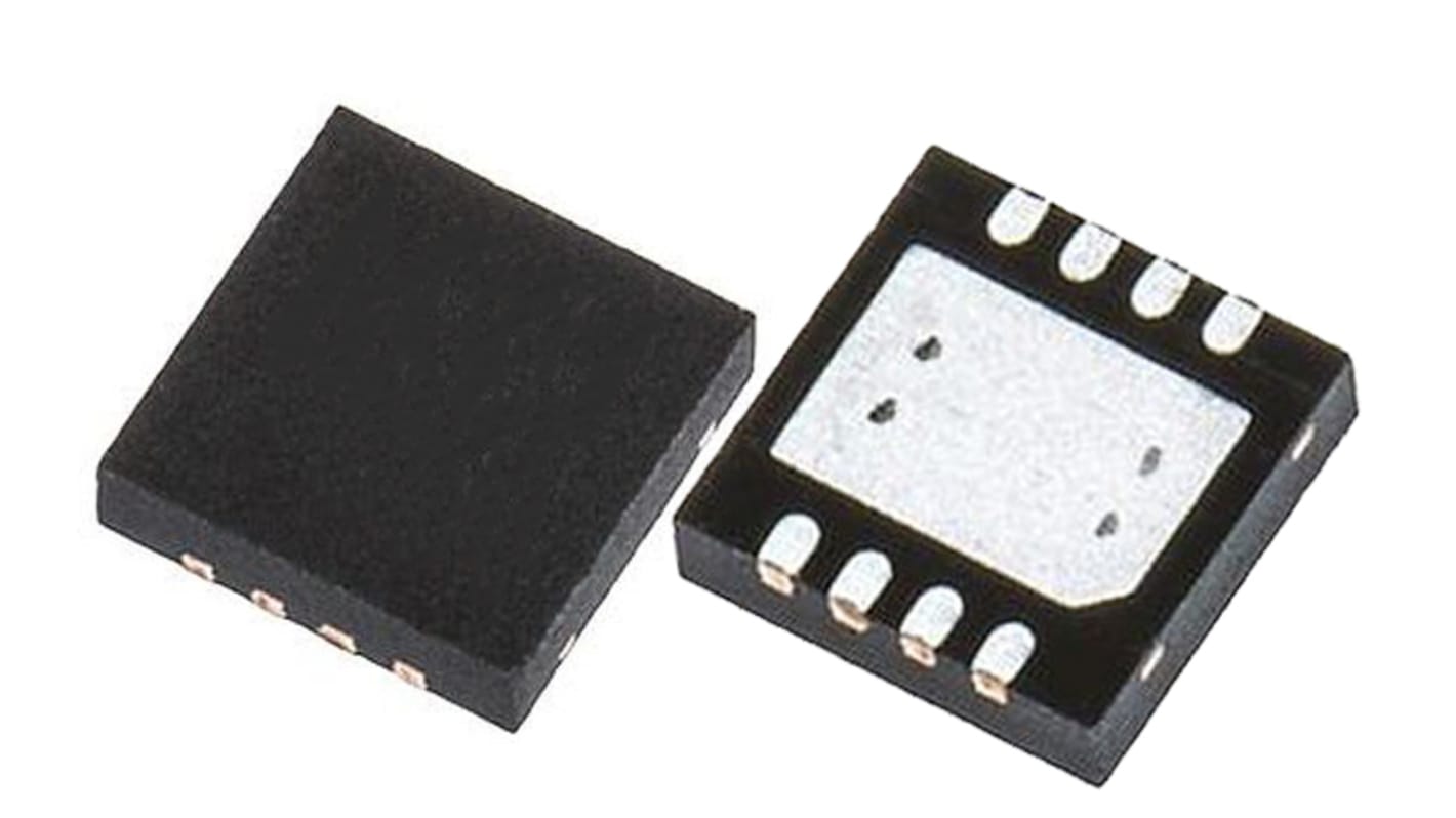
onsemi Type N-Channel MOSFET, 337 A, 80 V Enhancement, 8-Pin DFN NVMTS1D2N08H
- RS Stock No.:
- 195-2677
- Mfr. Part No.:
- NVMTS1D2N08H
- Brand:
- onsemi

Currently unavailable
Sorry, we don't know when this will be back in stock.
- RS Stock No.:
- 195-2677
- Mfr. Part No.:
- NVMTS1D2N08H
- Brand:
- onsemi
Specifications
Technical Reference
Legislation and Compliance
Product Details
Find similar products by selecting one or more attributes.
Select all | Attribute | Value |
|---|---|---|
| Brand | onsemi | |
| Channel Type | Type N | |
| Product Type | MOSFET | |
| Maximum Continuous Drain Current Id | 337A | |
| Maximum Drain Source Voltage Vds | 80V | |
| Package Type | DFN | |
| Mount Type | Surface | |
| Pin Count | 8 | |
| Maximum Drain Source Resistance Rds | 1.1mΩ | |
| Channel Mode | Enhancement | |
| Typical Gate Charge Qg @ Vgs | 147nC | |
| Minimum Operating Temperature | -55°C | |
| Maximum Power Dissipation Pd | 300W | |
| Maximum Operating Temperature | 175°C | |
| Length | 8.1mm | |
| Height | 1.15mm | |
| Standards/Approvals | No | |
| Automotive Standard | AEC-Q101 | |
| Select all | ||
|---|---|---|
Brand onsemi | ||
Channel Type Type N | ||
Product Type MOSFET | ||
Maximum Continuous Drain Current Id 337A | ||
Maximum Drain Source Voltage Vds 80V | ||
Package Type DFN | ||
Mount Type Surface | ||
Pin Count 8 | ||
Maximum Drain Source Resistance Rds 1.1mΩ | ||
Channel Mode Enhancement | ||
Typical Gate Charge Qg @ Vgs 147nC | ||
Minimum Operating Temperature -55°C | ||
Maximum Power Dissipation Pd 300W | ||
Maximum Operating Temperature 175°C | ||
Length 8.1mm | ||
Height 1.15mm | ||
Standards/Approvals No | ||
Automotive Standard AEC-Q101 | ||
Automotive Power MOSFET in a 8x8mm flat lead package designed for compact and efficient designs and including high thermal performance. Wettable Flank capable for Enhanced Optical Inspection. MOSFET and PPAP capable suitable for automotive applications.
Small Footprint (8x8 mm)
Compact Design
Low RDS(on)
Minimize Conduction Losses
Low QG and Capacitance
Minimize Driver Losses
Wettable Flank Option
Enhanced Optical Inspection
PPAP Capable
Application
Reverser Battery protection
Power switches (High Side Driver, Low Side Driver, H-Bridges etc.)
Related links
- onsemi Type N-Channel MOSFET 80 V Enhancement, 8-Pin DFN
- onsemi NTMFS0D8N Type N-Channel MOSFET 30 V Enhancement, 8-Pin DFN
- onsemi NTMFS0D8N Type N-Channel MOSFET 30 V Enhancement, 8-Pin DFN NTMFS0D8N03CT1G
- Vishay SiR N channel-Channel MOSFET 25 V Enhancement, 8-Pin PowerPAK SO-8 SiRA20DDP
- onsemi Type N-Channel MOSFET 40 V Enhancement, 8-Pin DFN
- onsemi Type N-Channel MOSFET 60 V Enhancement, 8-Pin DFN
- onsemi Type N-Channel MOSFET 40 V Enhancement, 8-Pin DFN
- onsemi Type N-Channel MOSFET 40 V Enhancement, 8-Pin DFN