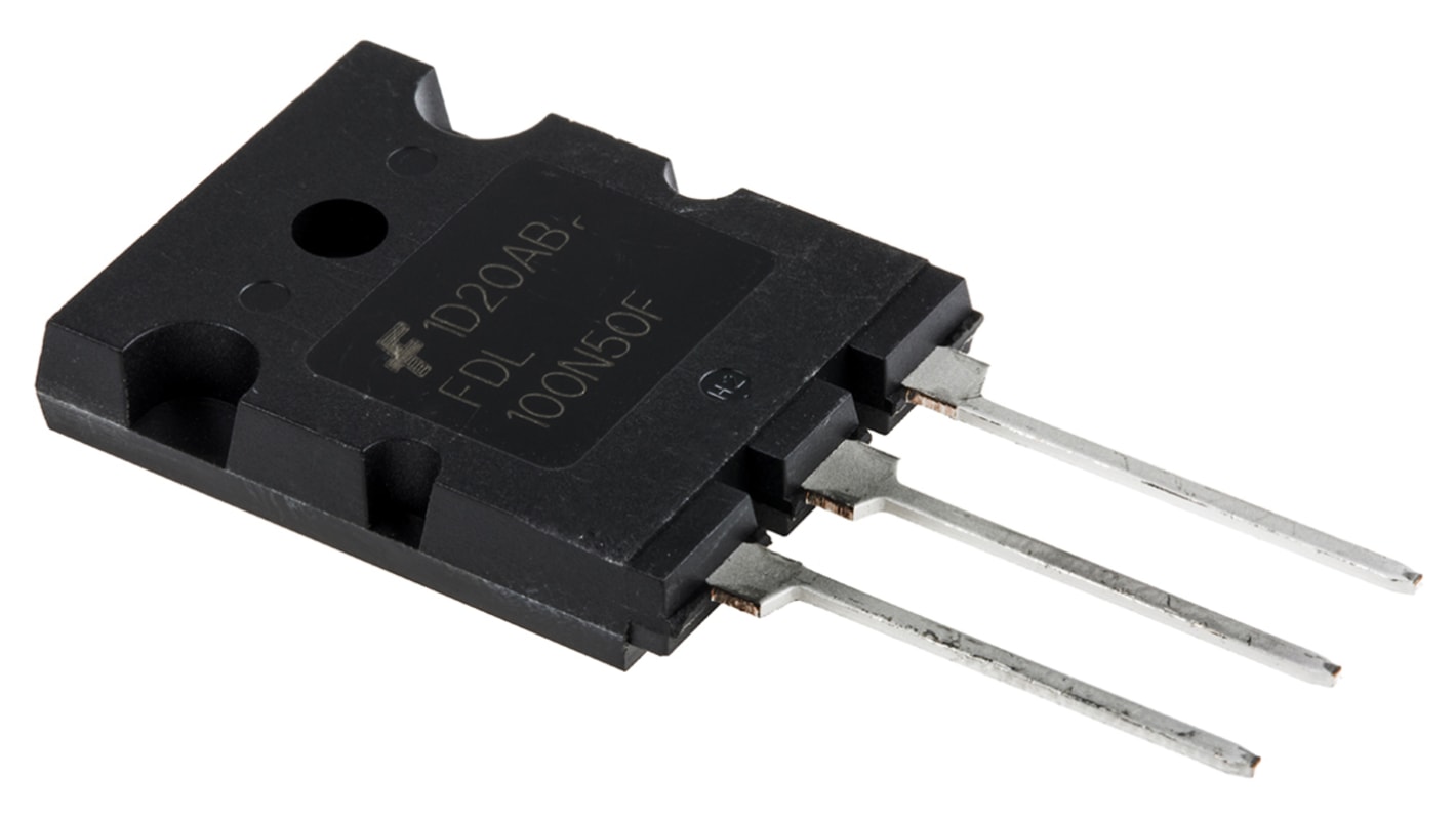
onsemi UniFET Type N-Channel MOSFET, 100 A, 500 V Enhancement, 3-Pin TO-264
- RS Stock No.:
- 124-1331
- Mfr. Part No.:
- FDL100N50F
- Brand:
- onsemi

Subtotal (1 tube of 25 units)*
£237.90
(exc. VAT)
£285.475
(inc. VAT)
FREE delivery for orders over £60.00
In Stock
- Plus 400 unit(s) shipping from 13 July 2026
Need more? Click ‘Check delivery dates’ to find extra stock and lead times.
Units | Per unit | Per Tube* |
|---|---|---|
| 25 + | £9.516 | £237.90 |
*price indicative
- RS Stock No.:
- 124-1331
- Mfr. Part No.:
- FDL100N50F
- Brand:
- onsemi
Specifications
Technical Reference
Legislation and Compliance
Product Details
Find similar products by selecting one or more attributes.
Select all | Attribute | Value |
|---|---|---|
| Brand | onsemi | |
| Product Type | MOSFET | |
| Channel Type | Type N | |
| Maximum Continuous Drain Current Id | 100A | |
| Maximum Drain Source Voltage Vds | 500V | |
| Series | UniFET | |
| Package Type | TO-264 | |
| Mount Type | Through Hole | |
| Pin Count | 3 | |
| Maximum Drain Source Resistance Rds | 55mΩ | |
| Channel Mode | Enhancement | |
| Maximum Power Dissipation Pd | 2.5kW | |
| Minimum Operating Temperature | -55°C | |
| Forward Voltage Vf | 1.5V | |
| Typical Gate Charge Qg @ Vgs | 238nC | |
| Maximum Operating Temperature | 150°C | |
| Length | 20mm | |
| Height | 20mm | |
| Standards/Approvals | No | |
| Automotive Standard | No | |
| Select all | ||
|---|---|---|
Brand onsemi | ||
Product Type MOSFET | ||
Channel Type Type N | ||
Maximum Continuous Drain Current Id 100A | ||
Maximum Drain Source Voltage Vds 500V | ||
Series UniFET | ||
Package Type TO-264 | ||
Mount Type Through Hole | ||
Pin Count 3 | ||
Maximum Drain Source Resistance Rds 55mΩ | ||
Channel Mode Enhancement | ||
Maximum Power Dissipation Pd 2.5kW | ||
Minimum Operating Temperature -55°C | ||
Forward Voltage Vf 1.5V | ||
Typical Gate Charge Qg @ Vgs 238nC | ||
Maximum Operating Temperature 150°C | ||
Length 20mm | ||
Height 20mm | ||
Standards/Approvals No | ||
Automotive Standard No | ||
UniFET™ N-Channel MOSFET, Fairchild Semiconductor
UniFET™ MOSFET is Fairchild Semiconductor's high voltage MOSFET family. It has the smallest on-state resistance among the Planar MOSFETs, and also provides superior switching performance and higher avalanche energy strength. In addition, the internal gate-source ESD diode allows UniFET-II™ MOSFET to withstand over 2000V HBM surge stress.
UniFET™ MOSFETs are suitable for switching power converter applications, such as power factor correction (PFC), flat panel display (FPD) TV power, ATX (Advanced Technology eXtended) and electronic lamp ballasts.
MOSFET Transistors, ON Semi
ON Semi offers a substantial portfolio of MOSFET devices that includes high-voltage (>250V) and low-voltage (<250V) types. The Advanced silicon technology provides smaller die sizes, which it is incorporated into multiple industry-standard and thermally-enhanced packages.
ON Semi MOSFETs provide superior design reliability from reduced voltage spikes and overshoot, to lower junction capacitance and reverse recovery charge, to elimination of additional external components to keep systems up and running longer.
Related links
- onsemi UniFET Type N-Channel MOSFET 500 V Enhancement, 3-Pin TO-264 FDL100N50F
- onsemi UniFET Type N-Channel MOSFET 500 V Enhancement, 3-Pin TO-247
- onsemi UniFET Type N-Channel MOSFET 500 V Enhancement, 3-Pin TO-220
- onsemi UniFET Type N-Channel MOSFET 500 V Enhancement, 3-Pin TO-263
- onsemi UniFET Type N-Channel MOSFET 500 V Enhancement, 3-Pin TO-220
- onsemi UniFET Type N-Channel MOSFET 500 V Enhancement, 3-Pin TO-220 FDP22N50N
- onsemi UniFET Type N-Channel MOSFET 500 V Enhancement, 3-Pin TO-220F FDPF5N50T
- onsemi UniFET Type N-Channel MOSFET 500 V Enhancement, 3-Pin TO-247 FDH44N50