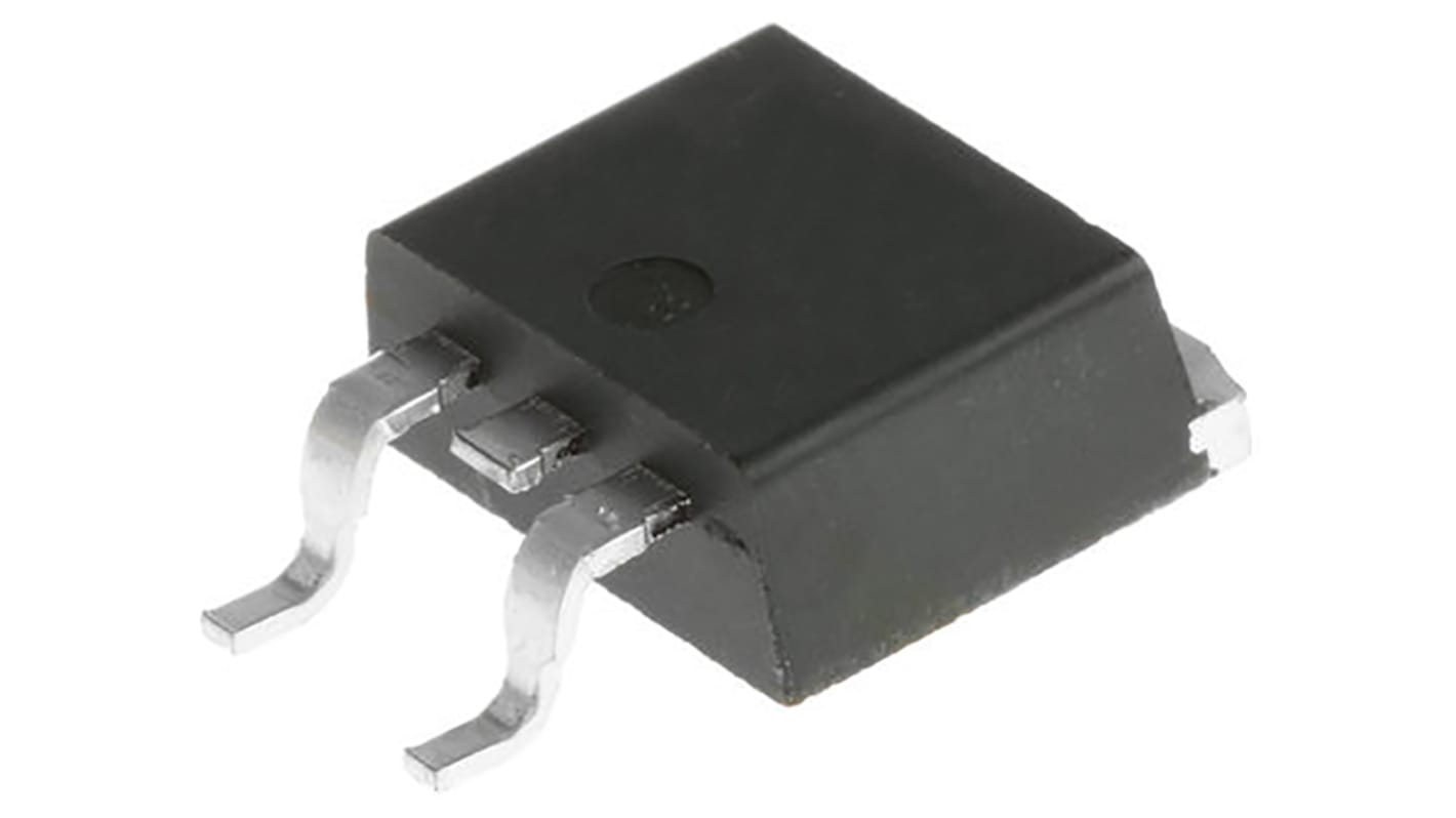
Infineon HEXFET Type N-Channel MOSFET, 43 A, 60 V Enhancement, 3-Pin TO-263 IRFS3806TRLPBF
- RS Stock No.:
- 827-4101
- Mfr. Part No.:
- IRFS3806TRLPBF
- Brand:
- Infineon

Bulk discount available
View bulk pricing optionsSubtotal (1 pack of 10 units)*
£8.82
(exc. VAT)
£10.58
(inc. VAT)
FREE delivery for orders over £60.00
In Stock
- Plus 1,340 unit(s) shipping from 13 July 2026
Need more? Click ‘Check delivery dates’ to find extra stock and lead times.
Units | Per unit | Per Pack* |
|---|---|---|
| 10 - 40 | £0.882 | £8.82 |
| 50 - 90 | £0.837 | £8.37 |
| 100 - 240 | £0.802 | £8.02 |
| 250 - 490 | £0.767 | £7.67 |
| 500 + | £0.484 | £4.84 |
*price indicative
- RS Stock No.:
- 827-4101
- Mfr. Part No.:
- IRFS3806TRLPBF
- Brand:
- Infineon
Specifications
Technical Reference
Legislation and Compliance
Product Details
Find similar products by selecting one or more attributes.
Select all | Attribute | Value |
|---|---|---|
| Brand | Infineon | |
| Product Type | MOSFET | |
| Channel Type | Type N | |
| Maximum Continuous Drain Current Id | 43A | |
| Maximum Drain Source Voltage Vds | 60V | |
| Package Type | TO-263 | |
| Series | HEXFET | |
| Mount Type | Surface | |
| Pin Count | 3 | |
| Maximum Drain Source Resistance Rds | 15.8mΩ | |
| Channel Mode | Enhancement | |
| Typical Gate Charge Qg @ Vgs | 22nC | |
| Maximum Power Dissipation Pd | 71W | |
| Minimum Operating Temperature | -55°C | |
| Forward Voltage Vf | 1.3V | |
| Maximum Operating Temperature | 175°C | |
| Standards/Approvals | No | |
| Height | 4.83mm | |
| Length | 10.67mm | |
| Automotive Standard | No | |
| Select all | ||
|---|---|---|
Brand Infineon | ||
Product Type MOSFET | ||
Channel Type Type N | ||
Maximum Continuous Drain Current Id 43A | ||
Maximum Drain Source Voltage Vds 60V | ||
Package Type TO-263 | ||
Series HEXFET | ||
Mount Type Surface | ||
Pin Count 3 | ||
Maximum Drain Source Resistance Rds 15.8mΩ | ||
Channel Mode Enhancement | ||
Typical Gate Charge Qg @ Vgs 22nC | ||
Maximum Power Dissipation Pd 71W | ||
Minimum Operating Temperature -55°C | ||
Forward Voltage Vf 1.3V | ||
Maximum Operating Temperature 175°C | ||
Standards/Approvals No | ||
Height 4.83mm | ||
Length 10.67mm | ||
Automotive Standard No | ||
- COO (Country of Origin):
- CN
Infineon HEXFET Series MOSFET, 43A Maximum Continuous Drain Current, 71W Maximum Power Dissipation - IRFS3806TRLPBF
This MOSFET is crafted for optimal performance in high-efficiency applications. Its enhancement mode configuration is pivotal in power management, driving significant usage across diverse electronic systems. It supports efficient switching and signal amplification, essential for sectors such as automation, electronics, and the electrical and mechanical industries.
Features & Benefits
• High continuous drain current capability of up to 43A
• Efficient operation with a maximum drain-source voltage of 60V
• Low on-resistance reduces power loss
• High-temperature application suitability with a range up to +175°C
• Space-saving surface mount design
• Enhanced ruggedness against dynamic stress for consistent performance
Applications
• Ideal for high-speed power switching scenarios
• Used in uninterruptible power supply systems
• Applicable in synchronous rectification within switched-mode power supplies
• Suitable for hard-switched and high-frequency circuits
What is the maximum gate-to-source voltage?
The maximum gate-to-source voltage for this component is -20V to +20V, allowing flexibility in various circuit designs.
How does the on-resistance affect power dissipation?
Lower on-resistance minimises power dissipation during operation, leading to enhanced efficiency and thermal performance.
What is the typical gate charge required?
The typical gate charge at a gate-source voltage of 10V is 22nC, enabling quick switching transitions.
Is it compatible with surface mount PCB designs?
Yes, the surface mount design is suitable for modern PCB layouts, facilitating integration into Compact electronic devices.
What factors should be considered when using the MOSFET in high-temperature applications?
When operating at high temperatures, ensure adequate thermal management is implemented to respect the maximum operating temperature limit of +175°C for reliability.

Related links
- Infineon HEXFET Type N-Channel MOSFET 60 V Enhancement, 3-Pin TO-263
- Infineon HEXFET Type N-Channel MOSFET 60 V Enhancement, 3-Pin TO-220 IRFB3806PBF
- Infineon HEXFET Type N-Channel MOSFET 60 V Enhancement, 3-Pin TO-220
- Infineon HEXFET Type N-Channel MOSFET 43 V Enhancement, 3-Pin TO-247
- Infineon HEXFET Type N-Channel MOSFET 43 V Enhancement, 3-Pin TO-247 IRFP3415PBF
- Infineon HEXFET Type N-Channel MOSFET 60 V TO-252
- Infineon HEXFET Type N-Channel MOSFET 150 V Enhancement, 3-Pin TO-220
- Infineon HEXFET Type N-Channel MOSFET 100 V Enhancement, 3-Pin TO-220