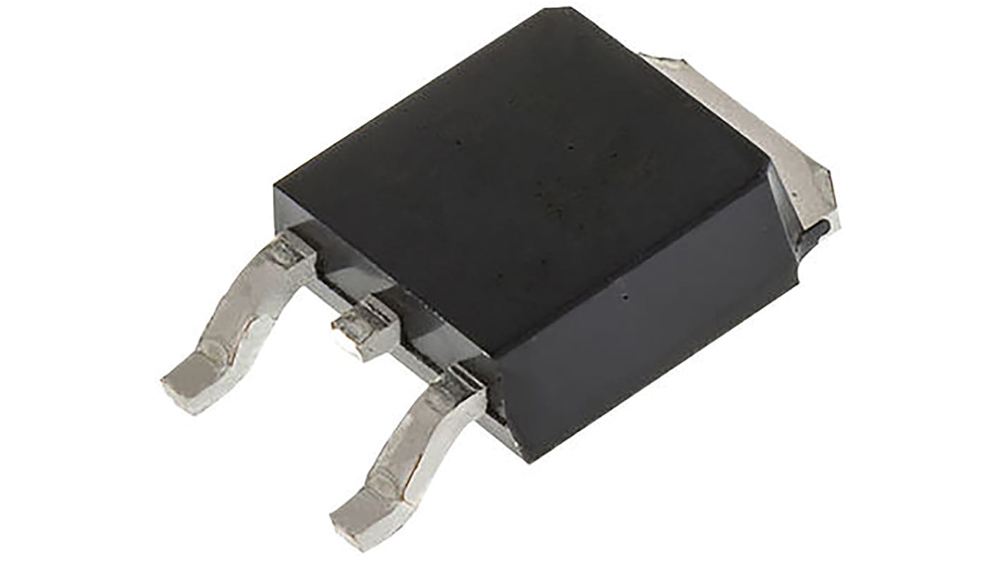
onsemi P-Channel MOSFET, 5.4 A, 60 V, 3-Pin DPAK FQD7P06TM
- RS Stock No.:
- 671-1030
- Mfr. Part No.:
- FQD7P06TM
- Brand:
- onsemi

Unavailable
RS will no longer stock this product.
- RS Stock No.:
- 671-1030
- Mfr. Part No.:
- FQD7P06TM
- Brand:
- onsemi
Specifications
Technical Reference
Legislation and Compliance
Find similar products by selecting one or more attributes.
Select all | Attribute | Value |
|---|---|---|
| Brand | onsemi | |
| Channel Type | P | |
| Maximum Continuous Drain Current | 5.4 A | |
| Maximum Drain Source Voltage | 60 V | |
| Package Type | DPAK (TO-252) | |
| Mounting Type | Surface Mount | |
| Pin Count | 3 | |
| Maximum Drain Source Resistance | 451 mΩ | |
| Channel Mode | Enhancement | |
| Minimum Gate Threshold Voltage | 2V | |
| Maximum Power Dissipation | 2.5 W | |
| Transistor Configuration | Single | |
| Maximum Gate Source Voltage | -25 V, +25 V | |
| Width | 6.22mm | |
| Typical Gate Charge @ Vgs | 6.3 nC @ 10 V | |
| Length | 6.73mm | |
| Number of Elements per Chip | 1 | |
| Transistor Material | Si | |
| Maximum Operating Temperature | +150 °C | |
| Height | 2.39mm | |
| Minimum Operating Temperature | -55 °C | |
| Select all | ||
|---|---|---|
Brand onsemi | ||
Channel Type P | ||
Maximum Continuous Drain Current 5.4 A | ||
Maximum Drain Source Voltage 60 V | ||
Package Type DPAK (TO-252) | ||
Mounting Type Surface Mount | ||
Pin Count 3 | ||
Maximum Drain Source Resistance 451 mΩ | ||
Channel Mode Enhancement | ||
Minimum Gate Threshold Voltage 2V | ||
Maximum Power Dissipation 2.5 W | ||
Transistor Configuration Single | ||
Maximum Gate Source Voltage -25 V, +25 V | ||
Width 6.22mm | ||
Typical Gate Charge @ Vgs 6.3 nC @ 10 V | ||
Length 6.73mm | ||
Number of Elements per Chip 1 | ||
Transistor Material Si | ||
Maximum Operating Temperature +150 °C | ||
Height 2.39mm | ||
Minimum Operating Temperature -55 °C | ||
Related links
- onsemi P-Channel MOSFET 60 V, 3-Pin D2PAK FQB47P06TM-AM002
- onsemi P-Channel MOSFET 75 V, 3-Pin D2PAK SMP3003-DL-1E
- onsemi P-Channel MOSFET 30 V, 3-Pin SC-70 3LP01M-TL-H
- Vishay TrenchFET N channel-Channel MOSFET 60 V Enhancement, 8-Pin SO-8 SQ9945CEY-T1_GE3
- Infineon HEXFET Type P-Channel MOSFET 30 V Enhancement, 8-Pin SOIC
- Infineon HEXFET Type P-Channel MOSFET 30 V Enhancement, 8-Pin SOIC IRF9335TRPBF
- Vishay TrenchFET Type P-Channel MOSFET 80 V Enhancement, 6-Pin TSOP Si3129DV-T1-GE3
- Vishay TrenchFET Type P-Channel MOSFET 80 V Enhancement, 6-Pin TSOP
