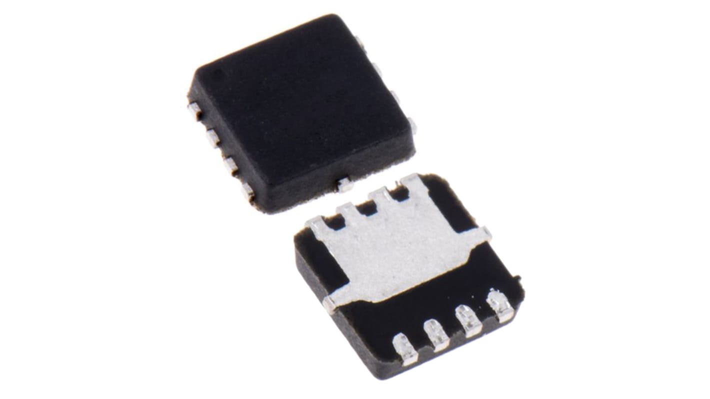
onsemi NTTFS6H850N Type N-Channel MOSFET, 68 A, 80 V Enhancement, 8-Pin WDFN
- RS Stock No.:
- 178-4439P
- Mfr. Part No.:
- NTTFS6H850NTAG
- Brand:
- onsemi

Bulk discount available
Subtotal 100 units (supplied on a continuous strip)*
£65.20
(exc. VAT)
£78.20
(inc. VAT)
FREE delivery for orders over £60.00
Temporarily out of stock
- Shipping from 25 November 2026
Need more? Click ‘Check delivery dates’ to find extra stock and lead times.
Units | Per unit |
|---|---|
| 100 - 240 | £0.652 |
| 250 - 490 | £0.635 |
| 500 - 990 | £0.556 |
| 1000 + | £0.472 |
*price indicative
- RS Stock No.:
- 178-4439P
- Mfr. Part No.:
- NTTFS6H850NTAG
- Brand:
- onsemi
Specifications
Technical Reference
Legislation and Compliance
Product Details
Find similar products by selecting one or more attributes.
Select all | Attribute | Value |
|---|---|---|
| Brand | onsemi | |
| Product Type | MOSFET | |
| Channel Type | Type N | |
| Maximum Continuous Drain Current Id | 68A | |
| Maximum Drain Source Voltage Vds | 80V | |
| Package Type | WDFN | |
| Series | NTTFS6H850N | |
| Mount Type | Surface | |
| Pin Count | 8 | |
| Maximum Drain Source Resistance Rds | 9.5mΩ | |
| Channel Mode | Enhancement | |
| Maximum Power Dissipation Pd | 107W | |
| Typical Gate Charge Qg @ Vgs | 3.6nC | |
| Minimum Operating Temperature | -55°C | |
| Forward Voltage Vf | 1.2V | |
| Maximum Operating Temperature | 175°C | |
| Length | 3.15mm | |
| Height | 0.75mm | |
| Standards/Approvals | No | |
| Automotive Standard | No | |
| Select all | ||
|---|---|---|
Brand onsemi | ||
Product Type MOSFET | ||
Channel Type Type N | ||
Maximum Continuous Drain Current Id 68A | ||
Maximum Drain Source Voltage Vds 80V | ||
Package Type WDFN | ||
Series NTTFS6H850N | ||
Mount Type Surface | ||
Pin Count 8 | ||
Maximum Drain Source Resistance Rds 9.5mΩ | ||
Channel Mode Enhancement | ||
Maximum Power Dissipation Pd 107W | ||
Typical Gate Charge Qg @ Vgs 3.6nC | ||
Minimum Operating Temperature -55°C | ||
Forward Voltage Vf 1.2V | ||
Maximum Operating Temperature 175°C | ||
Length 3.15mm | ||
Height 0.75mm | ||
Standards/Approvals No | ||
Automotive Standard No | ||
- COO (Country of Origin):
- MY
Commercial Power MOSFET in a 3x3mm flat lead package designed for compact and efficient designs and including high thermal performance.
Features
Low On-Resistance
Low Gate Charge
Small Footprint (3x3 mm)
Benefits
Minimizes Conduction Losses
Minimizes Switching Losses
Compact Design
Applications
Reverser Battery protection
Power switches (High Side Driver, Low Side Driver, H-Bridges etc.)
Synchronous Rectification
End Products
Motor Control
Battery management
Switching Power supplies