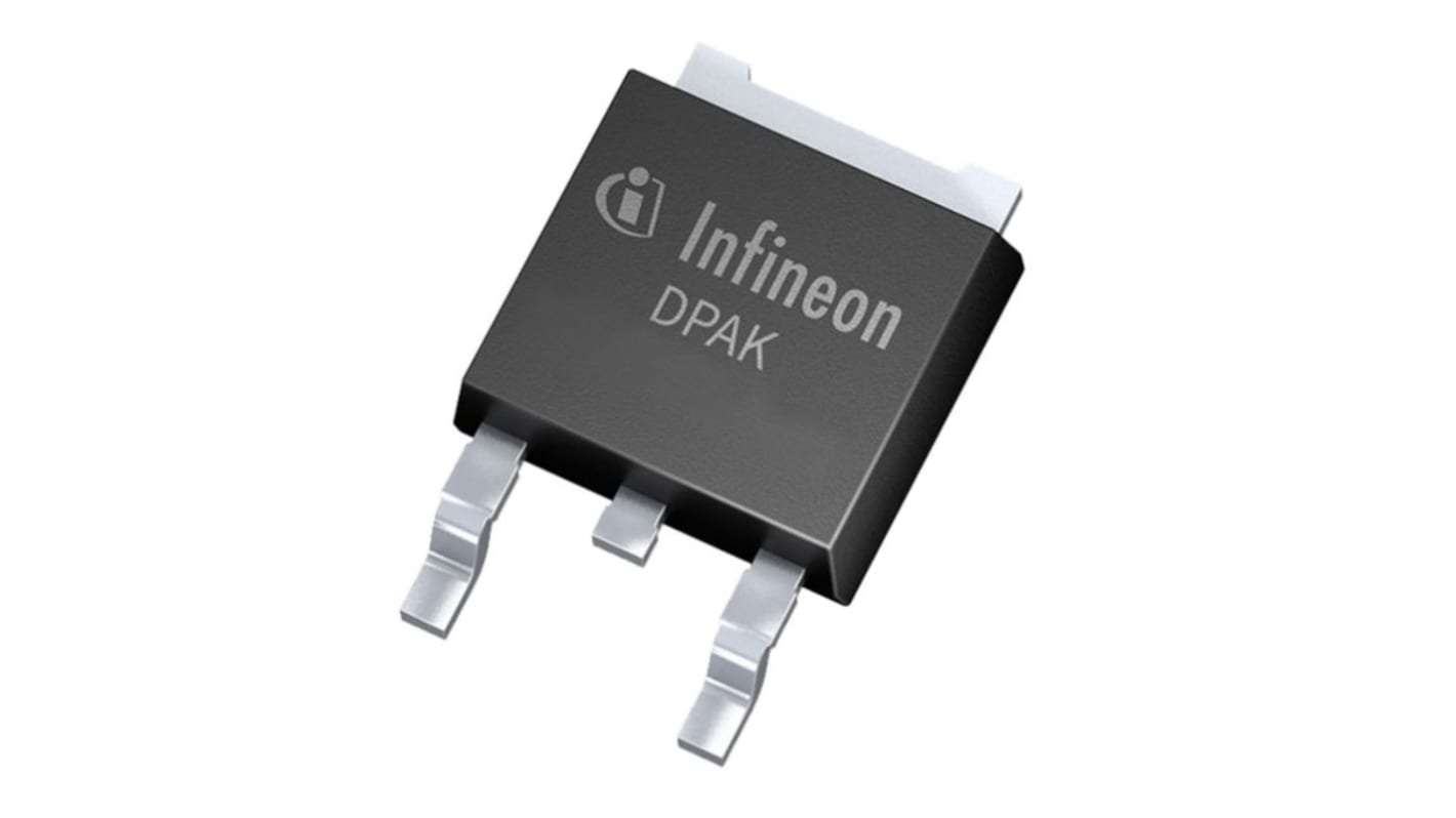
Infineon OptiMOS™ 3 N-Channel MOSFET, 90 A, 100 V, 3-Pin DPAK IPD068N10N3GATMA1
- RS Stock No.:
- 171-1939P
- Mfr. Part No.:
- IPD068N10N3GATMA1
- Brand:
- Infineon

Subtotal 100 units (supplied on a continuous strip)*
£51.40
(exc. VAT)
£61.70
(inc. VAT)
FREE delivery for orders over £50.00
- 17,880 unit(s) ready to ship
Units | Per unit |
|---|---|
| 100 - 240 | £0.514 |
| 250 - 490 | £0.489 |
| 500 - 990 | £0.449 |
| 1000 + | £0.371 |
*price indicative
- RS Stock No.:
- 171-1939P
- Mfr. Part No.:
- IPD068N10N3GATMA1
- Brand:
- Infineon
Select all | Attribute | Value |
|---|---|---|
| Brand | Infineon | |
| Channel Type | N | |
| Maximum Continuous Drain Current | 90 A | |
| Maximum Drain Source Voltage | 100 V | |
| Package Type | TO-252 | |
| Series | OptiMOS™ 3 | |
| Mounting Type | Surface Mount | |
| Pin Count | 3 | |
| Maximum Drain Source Resistance | 12.3 mΩ | |
| Channel Mode | Enhancement | |
| Maximum Gate Threshold Voltage | 3.5V | |
| Minimum Gate Threshold Voltage | 2V | |
| Maximum Power Dissipation | 150 W | |
| Transistor Configuration | Single | |
| Maximum Gate Source Voltage | 20 V | |
| Width | 7.47mm | |
| Typical Gate Charge @ Vgs | 51 nC @ 10 V | |
| Length | 6.73mm | |
| Number of Elements per Chip | 1 | |
| Maximum Operating Temperature | +175 °C | |
| Height | 2.41mm | |
| Minimum Operating Temperature | -55 °C | |
| Forward Diode Voltage | 1.2V | |
| Select all | ||
|---|---|---|
Brand Infineon | ||
Channel Type N | ||
Maximum Continuous Drain Current 90 A | ||
Maximum Drain Source Voltage 100 V | ||
Package Type TO-252 | ||
Series OptiMOS™ 3 | ||
Mounting Type Surface Mount | ||
Pin Count 3 | ||
Maximum Drain Source Resistance 12.3 mΩ | ||
Channel Mode Enhancement | ||
Maximum Gate Threshold Voltage 3.5V | ||
Minimum Gate Threshold Voltage 2V | ||
Maximum Power Dissipation 150 W | ||
Transistor Configuration Single | ||
Maximum Gate Source Voltage 20 V | ||
Width 7.47mm | ||
Typical Gate Charge @ Vgs 51 nC @ 10 V | ||
Length 6.73mm | ||
Number of Elements per Chip 1 | ||
Maximum Operating Temperature +175 °C | ||
Height 2.41mm | ||
Minimum Operating Temperature -55 °C | ||
Forward Diode Voltage 1.2V | ||
RoHS Status: Not Applicable
Infineon OptiMOS™3 Power MOSFETs, 100V and over
Infineon MOSFET
Features and Benefits
• Environmentally friendly
• Excellent gate charge x RDS (on) product (FOM)
• Excellent switching performance
• Halogen free
• Highest power density
• Increased efficiency
• Lead (Pb) free plating
• Less paralleling required
• Operating temperature ranges between -55°C and 175°C
• Smallest board space consumption
• Very low Qg and Qgd
• World's lowest RDS (on)
Applications
• Isolated DC-DC converters (telecom and data communication systems
• Motor control for 48V-80V systems (domestic vehicles, power tools, trucks)
• O-ring switches and circuit breakers in 48V systems
• Synchronous rectifier
Certifications
• BS EN 61340-5-1:2007
• IEC61249-2-21
• JEDEC


