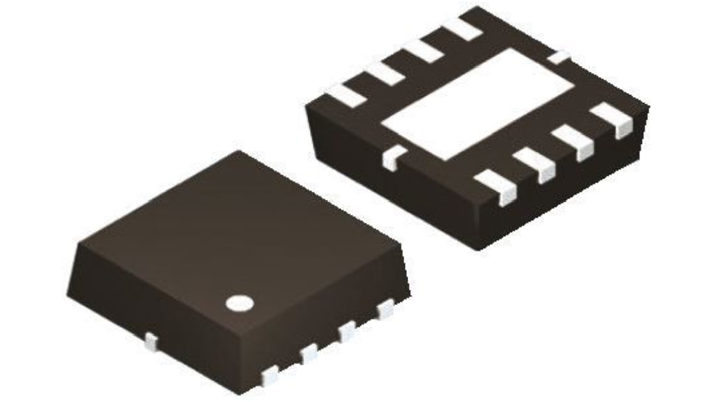
onsemi Series PowerTrench 2 Type N-Channel MOSFET, 26 A, 30 V Enhancement, 8-Pin WDFN
- RS Stock No.:
- 166-1727
- Mfr. Part No.:
- FDPC8013S
- Brand:
- onsemi

Subtotal (1 reel of 3000 units)*
£2,130.00
(exc. VAT)
£2,550.00
(inc. VAT)
FREE delivery for orders over £60.00
Temporarily out of stock
- Shipping from 23 November 2026
Need more? Click ‘Check delivery dates’ to find extra stock and lead times.
Units | Per unit | Per Reel* |
|---|---|---|
| 3000 + | £0.71 | £2,130.00 |
*price indicative
- RS Stock No.:
- 166-1727
- Mfr. Part No.:
- FDPC8013S
- Brand:
- onsemi
Specifications
Technical Reference
Legislation and Compliance
Product Details
Find similar products by selecting one or more attributes.
Select all | Attribute | Value |
|---|---|---|
| Brand | onsemi | |
| Channel Type | Type N | |
| Product Type | MOSFET | |
| Maximum Continuous Drain Current Id | 26A | |
| Maximum Drain Source Voltage Vds | 30V | |
| Series | PowerTrench | |
| Package Type | WDFN | |
| Mount Type | Surface | |
| Pin Count | 8 | |
| Maximum Drain Source Resistance Rds | 9.2mΩ | |
| Channel Mode | Enhancement | |
| Minimum Operating Temperature | -55°C | |
| Typical Gate Charge Qg @ Vgs | 13nC | |
| Forward Voltage Vf | 0.8V | |
| Maximum Power Dissipation Pd | 2W | |
| Maximum Operating Temperature | 150°C | |
| Transistor Configuration | Series | |
| Length | 3.4mm | |
| Standards/Approvals | No | |
| Height | 0.75mm | |
| Number of Elements per Chip | 2 | |
| Automotive Standard | No | |
| Select all | ||
|---|---|---|
Brand onsemi | ||
Channel Type Type N | ||
Product Type MOSFET | ||
Maximum Continuous Drain Current Id 26A | ||
Maximum Drain Source Voltage Vds 30V | ||
Series PowerTrench | ||
Package Type WDFN | ||
Mount Type Surface | ||
Pin Count 8 | ||
Maximum Drain Source Resistance Rds 9.2mΩ | ||
Channel Mode Enhancement | ||
Minimum Operating Temperature -55°C | ||
Typical Gate Charge Qg @ Vgs 13nC | ||
Forward Voltage Vf 0.8V | ||
Maximum Power Dissipation Pd 2W | ||
Maximum Operating Temperature 150°C | ||
Transistor Configuration Series | ||
Length 3.4mm | ||
Standards/Approvals No | ||
Height 0.75mm | ||
Number of Elements per Chip 2 | ||
Automotive Standard No | ||
- COO (Country of Origin):
- MY
PowerTrench® Dual N-Channel MOSFET, Fairchild Semiconductor
ON Semis PowerTrench® MOSFETS are optimised power switched that offer increased system efficiency and power density. They combine small gate charge, small reverse recovery and a soft reverse recovery body diode to contribute to fast switching of synchronous rectification in AC/DC power supplies.
The soft body diode performance of the PowerTrench® MOSFETs is able to eliminate snubber circuit or replace a higher voltage rating MOSFET.
MOSFET Transistors, ON Semi
ON Semi offers a substantial portfolio of MOSFET devices that includes high-voltage (>250V) and low-voltage (<250V) types. The Advanced silicon technology provides smaller die sizes, which it is incorporated into multiple industry-standard and thermally-enhanced packages.
ON Semi MOSFETs provide superior design reliability from reduced voltage spikes and overshoot, to lower junction capacitance and reverse recovery charge, to elimination of additional external components to keep systems up and running longer.
Related links
- onsemi Series PowerTrench 2 Type N-Channel MOSFET 30 V Enhancement, 8-Pin WDFN FDPC8013S
- onsemi Isolated PowerTrench 16 A 8-Pin WDFN
- onsemi Isolated PowerTrench 16 A 8-Pin WDFN FDMC7208S
- onsemi PowerTrench Type N-Channel MOSFET 40 V Enhancement, 8-Pin WDFN
- onsemi PowerTrench Type N-Channel MOSFET 40 V Enhancement, 8-Pin WDFN
- onsemi PowerTrench Type N-Channel MOSFET 150 V Enhancement, 8-Pin WDFN
- onsemi PowerTrench Type N-Channel MOSFET 40 V Enhancement, 8-Pin WDFN
- onsemi PowerTrench Type N-Channel MOSFET 80 V Enhancement, 8-Pin WDFN