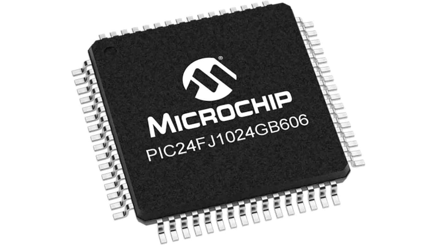
Microchip PIC24FJ1024GB606-I/PT, 16 bit 16 Bit CPU, PIC24FJ Microcontroller, 32 MHz, 1MB FLASH, 64-Pin QFP
- RS Stock No.:
- 151-1495
- Mfr. Part No.:
- PIC24FJ1024GB606-I/PT
- Brand:
- Microchip

Subtotal (1 pack of 2 units)*
£8.64
(exc. VAT)
£10.36
(inc. VAT)
FREE delivery for orders over £60.00
In Stock
- 326 unit(s) ready to ship
Need more? Click ‘Check delivery dates’ to find extra stock and lead times.
Units | Per unit | Per Pack* |
|---|---|---|
| 2 + | £4.32 | £8.64 |
*price indicative
- RS Stock No.:
- 151-1495
- Mfr. Part No.:
- PIC24FJ1024GB606-I/PT
- Brand:
- Microchip
Specifications
Technical Reference
Legislation and Compliance
Product Details
Find similar products by selecting one or more attributes.
Select all | Attribute | Value |
|---|---|---|
| Brand | Microchip | |
| Product Type | Microcontroller | |
| Series | PIC24FJ | |
| Package Type | QFP | |
| Mount Type | Surface | |
| Pin Count | 64 | |
| Device Core | 16 Bit CPU | |
| Data Bus Width | 16bit | |
| Program Memory Size | 1MB | |
| Maximum Clock Frequency | 32MHz | |
| RAM Size | 32kB | |
| Maximum Supply Voltage | 3.6V | |
| Analogue Comparators | 3 | |
| Minimum Operating Temperature | -40°C | |
| Maximum Operating Temperature | 85°C | |
| Standards/Approvals | No | |
| Height | 0.85mm | |
| Length | 9mm | |
| Minimum Supply Voltage | 2V | |
| Automotive Standard | No | |
| ADCs | 16 x 10/12 Bit | |
| Program Memory Type | FLASH | |
| Instruction Set Architecture | C Compiler | |
| Select all | ||
|---|---|---|
Brand Microchip | ||
Product Type Microcontroller | ||
Series PIC24FJ | ||
Package Type QFP | ||
Mount Type Surface | ||
Pin Count 64 | ||
Device Core 16 Bit CPU | ||
Data Bus Width 16bit | ||
Program Memory Size 1MB | ||
Maximum Clock Frequency 32MHz | ||
RAM Size 32kB | ||
Maximum Supply Voltage 3.6V | ||
Analogue Comparators 3 | ||
Minimum Operating Temperature -40°C | ||
Maximum Operating Temperature 85°C | ||
Standards/Approvals No | ||
Height 0.85mm | ||
Length 9mm | ||
Minimum Supply Voltage 2V | ||
Automotive Standard No | ||
ADCs 16 x 10/12 Bit | ||
Program Memory Type FLASH | ||
Instruction Set Architecture C Compiler | ||
The Microchip PIC24FJ1024GB606 microcontroller has C compiler optimized instruction Set architecture with large, dual partition flash program memory and USB On-The-Go (OTG). It includes up to 1MB of Flash memory with Error Correction Code (ECC) ,32 KB of RAM and USB connectivity. It operates on 2V to 3.6V voltage range. This device also features dual-partition Flash with Live Update capability, enabling them to hold two independent software applications, permitting simultaneous programming of one partition while executing application code from the other. It has 1024 flash program memory and 32K.data memory.
Up to 16 MIPS Operation @ 32 MHz
Two Address Generation Units for Separate Read and Write Addressing of Data Memory
10,000 Erase/Write Cycle Endurance, Typical
Data Retention of 20 Years Minimum
Self-Programmable under Software Control
On-Chip Voltage Regulators (1.8V) for Low-Power Operation
Programmable Reference Clock Output
In-Circuit Serial Programming™ (ICSP™) and In-Circuit Emulation (ICE) via Two Pins
JTAG Boundary Scan Support
Detects clock failure and switches to on-chip, low-power RC Oscillator
Power-on Reset (POR), Brown-out Reset (BOR), Power-up Timer (PWRT) and Oscillator Start-up Timer (OST)
Programmable High/Low-Voltage Detect (HLVD)
Flexible Watchdog Timer (WDT) with its Own RC Oscillator for Reliable Operation
Sleep and Idle modes Selectively Shut Down
Peripherals and/or Core for Substantial Power
Reduction and Fast Wake-up
Doze mode Allows CPU to Run at a Lower Clock Speed than Peripherals
Alternate Clock modes Allow On-the-Fly Switching to a Lower Clock Speed for Selective Power Reduction
Wide Range Digitally Controlled Oscillator (DCO) for Fast Start-up and Low-Power Operation
USB v2.0 On-The-Go (OTG) Compliant
Dual Role Capable – Can Act as Either Host or Peripheral
Low-Speed (1.5 Mb/s) and Full-Speed (12 Mb/s)
USB Operation in Host mode
Full-Speed USB Operation in Device mode
High-Precision PLL for USB
USB Device mode Operation from FRC Oscillator – No Crystal Oscillator Required
Temperature range between 40°C to +85°C
TQFP (Plastic Thin Quad Flatpack) package
Related links
- Microchip PIC24FJ Microcontroller 1MB FLASH, 64-Pin QFP
- Microchip PIC24FJ1024GA606-I/PT PIC24FJ Microcontroller 1MB FLASH, 64-Pin TQFP
- Microchip PIC24FJ Microcontroller 1MB FLASH, 64-Pin TQFP
- Microchip PIC24FJ1024GB610-I/PT PIC24FJ Microcontroller 1MB FLASH, 100-Pin TQFP
- Microchip PIC24FJ256GA606-I/PT PIC24F Microcontroller 1MB FLASH, 64-Pin TQFP
- Microchip PIC24FJ64GA306-I/PT PIC24FJ Microcontroller 64kB FLASH, 64-Pin TQFP
- Microchip PIC24FJ Microcontroller 1MB FLASH, 100-Pin TQFP
- Microchip PIC24FJ256GB206-I/PT PIC24FJ Microcontroller 256kB FLASH, 64-Pin TQFP
