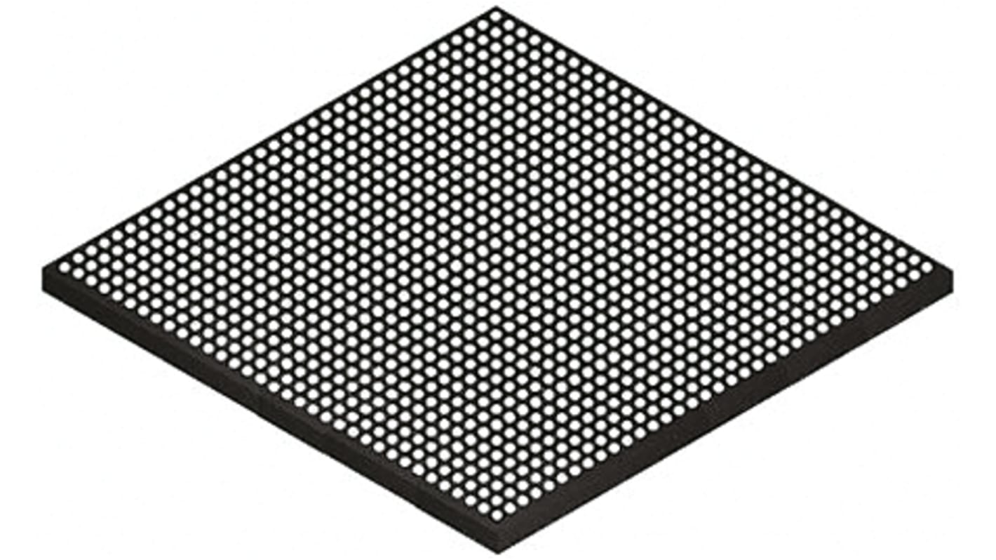
Altera FPGA 5AGXFB3H4F40C5N, Arria V 362000 Cells, 362k Gates, 19358kbit, 362000 Blocks, 1517-Pin FBGA
- RS Stock No.:
- 830-3590P
- Mfr. Part No.:
- 5AGXFB3H4F40C5N
- Brand:
- Altera

Unavailable
RS will no longer stock this product.
- RS Stock No.:
- 830-3590P
- Mfr. Part No.:
- 5AGXFB3H4F40C5N
- Brand:
- Altera
Specifications
Technical Reference
Legislation and Compliance
Product Details
Find similar products by selecting one or more attributes.
Select all | Attribute | Value |
|---|---|---|
| Brand | Altera | |
| Family Name | Arria V | |
| Number of Logic Gates | 362k | |
| Number of Logic Cells | 362000 | |
| Number of Logic Units | 362000 | |
| Dedicated DSP | Yes | |
| Number of Registers | 547520 | |
| Number of Multipliers | 1045 (27 x 27), 2090 (18 x 18), 3135 (9 x 9) | |
| Mounting Type | Surface Mount | |
| Package Type | FBGA | |
| Pin Count | 1517 | |
| Number of RAM Bits | 19358kbit | |
| Dimensions | 40 x 40 x 2.1mm | |
| Height | 2.1mm | |
| Length | 40mm | |
| Maximum Operating Temperature | +85 °C | |
| Maximum Operating Supply Voltage | 1.13 V | |
| Width | 40mm | |
| Minimum Operating Supply Voltage | 1.07 V | |
| Minimum Operating Temperature | 0 °C | |
| Select all | ||
|---|---|---|
Brand Altera | ||
Family Name Arria V | ||
Number of Logic Gates 362k | ||
Number of Logic Cells 362000 | ||
Number of Logic Units 362000 | ||
Dedicated DSP Yes | ||
Number of Registers 547520 | ||
Number of Multipliers 1045 (27 x 27), 2090 (18 x 18), 3135 (9 x 9) | ||
Mounting Type Surface Mount | ||
Package Type FBGA | ||
Pin Count 1517 | ||
Number of RAM Bits 19358kbit | ||
Dimensions 40 x 40 x 2.1mm | ||
Height 2.1mm | ||
Length 40mm | ||
Maximum Operating Temperature +85 °C | ||
Maximum Operating Supply Voltage 1.13 V | ||
Width 40mm | ||
Minimum Operating Supply Voltage 1.07 V | ||
Minimum Operating Temperature 0 °C | ||
Arria V GX FPGA with 6Gbps Transceivers, Altera
These devices Provide bandwidth, cost, and power levels that are optimized for high-volume data and signal-processing applications.
An FPGA is a semiconductor device consisting of a matrix of Configurable Logic Blocks (CLBs) connected through programmable interconnects. The user determines these interconnections by programming SRAM. A CLB can be simple (AND, OR gates, etc) or complex (a block of RAM). The FPGA allows changes to be made to a design even after the device is soldered into a PCB.
Related links
- Altera FPGA 5AGXFB3H4F40C5N 362k Gates 362000 Blocks, 1517-Pin FBGA
- Altera FPGA 5AGXFB3H4F35I5N 362k Gates 362000 Blocks, 1152-Pin FBGA
- Altera FPGA 5AGXMB1G4F40C4N 300k Gates 300000 Blocks, 1517-Pin FBGA
- Altera FPGA 5AGXBA1D6F27C6N 463 kbit 672-Pin FBGA
- Altera FPGA 5AGXMA1D6F31C6N 463 kbit 896-Pin FBGA
- Altera FPGA 5AGXBA7D6F31C6N 13660 kbit 896-Pin FBGA
- Altera FPGA 5AGXBA5D6F31C6N 1173 kbit 896-Pin FBGA
- Altera FPGA 5CEBA4 49000 Cells 3464192 bit 18480 Blocks, 256-Pin FBGA
