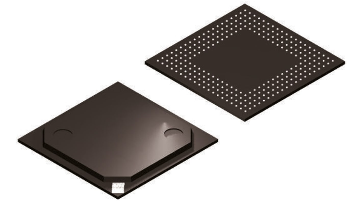
Altera FPGA EP4CE6F17C8LN Cyclone IV E 6272 Cells, 6272 Gates, 276480 bit 392 Blocks, 256-Pin FBGA
- RS Stock No.:
- 830-3537
- Mfr. Part No.:
- EP4CE6F17C8LN
- Brand:
- Altera

Subtotal (1 unit)*
£21.53
(exc. VAT)
£25.84
(inc. VAT)
FREE delivery for orders over £60.00
In Stock
- 12 unit(s) ready to ship
Need more? Click ‘Check delivery dates’ to find extra stock and lead times.
Units | Per unit |
|---|---|
| 1 + | £21.53 |
*price indicative
- RS Stock No.:
- 830-3537
- Mfr. Part No.:
- EP4CE6F17C8LN
- Brand:
- Altera
Specifications
Technical Reference
Legislation and Compliance
Product Details
Find similar products by selecting one or more attributes.
Select all | Attribute | Value |
|---|---|---|
| Brand | Altera | |
| Series | Cyclone IV E | |
| Product Type | FPGA | |
| Number of Logic Gates | 6272 | |
| Number of Logic Cells | 6272 | |
| Number of Logic Units | 392 | |
| Number of Multipliers | 360 (18 x 18) | |
| Mount Type | Surface | |
| Package Type | FBGA | |
| Minimum Supply Voltage | 0.97V | |
| Maximum Supply Voltage | 1.03V | |
| Pin Count | 256 | |
| Number of RAM Bits | 276480bit | |
| Minimum Operating Temperature | 0°C | |
| Maximum Operating Temperature | 85°C | |
| Standards/Approvals | No | |
| Length | 17mm | |
| Automotive Standard | No | |
| Select all | ||
|---|---|---|
Brand Altera | ||
Series Cyclone IV E | ||
Product Type FPGA | ||
Number of Logic Gates 6272 | ||
Number of Logic Cells 6272 | ||
Number of Logic Units 392 | ||
Number of Multipliers 360 (18 x 18) | ||
Mount Type Surface | ||
Package Type FBGA | ||
Minimum Supply Voltage 0.97V | ||
Maximum Supply Voltage 1.03V | ||
Pin Count 256 | ||
Number of RAM Bits 276480bit | ||
Minimum Operating Temperature 0°C | ||
Maximum Operating Temperature 85°C | ||
Standards/Approvals No | ||
Length 17mm | ||
Automotive Standard No | ||
Cyclone FPGA, Altera
An FPGA is a semiconductor device consisting of a Matrix of Configurable Logic Blocks (CLBs) connected through programmable interconnects. The user determines these interconnections by programming SRAM. A CLB can be simple (AND, OR gates, etc) or complex (a Block of RAM). The FPGA allows changes to be MADE to a design even after the device is soldered into a PCB.
Related links
- Altera FPGA Cyclone IV E 6272 Cells 276480 bit 392 Blocks, 256-Pin FBGA
- Altera FPGA Cyclone IV E 6272 Cells 276480 bit 392 Blocks, 144-Pin EQFP
- Altera FPGA EP4CE6E22I7N Cyclone IV E 6272 Cells 276480 bit 392 Blocks, 144-Pin EQFP
- Altera FPGA EP4CE6E22C8N Cyclone IV 6272 Cells 144-Pin EQFP
- Altera FPGA Cyclone IV 6272 Cells 144-Pin EQFP
- Altera FPGA Cyclone IV 28848 Cells 484-Pin FBGA
- Altera FPGA Cyclone IV GX 14400 Cells 169-Pin FBGA
- Altera FPGA EP4CE30F23C8N Cyclone IV 28848 Cells 484-Pin FBGA