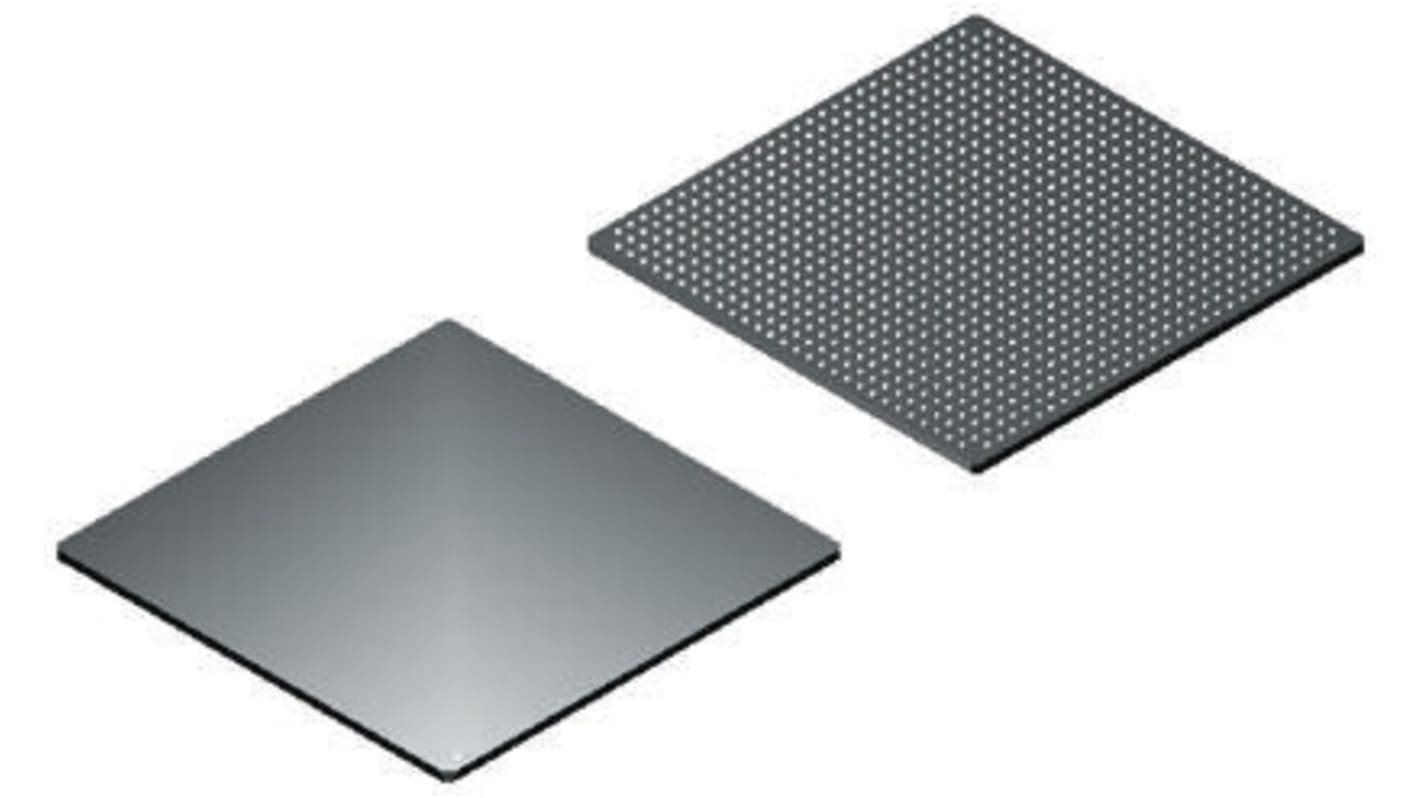
Altera FPGA 5AGXMA1D6F31C6N, Arria V 75000 Cells, 463 kbit, 8000 kbit, 896-Pin FBGA
- RS Stock No.:
- 790-7046
- Mfr. Part No.:
- 5AGXMA1D6F31C6N
- Brand:
- Altera

Bulk discount available
Subtotal (1 unit)*
£193.89
(exc. VAT)
£232.67
(inc. VAT)
Stock information currently inaccessible
Units | Per unit |
|---|---|
| 1 - 4 | £193.89 |
| 5 + | £191.34 |
*price indicative
- RS Stock No.:
- 790-7046
- Mfr. Part No.:
- 5AGXMA1D6F31C6N
- Brand:
- Altera
Specifications
Technical Reference
Legislation and Compliance
Product Details
Find similar products by selecting one or more attributes.
Select all | Attribute | Value |
|---|---|---|
| Brand | Altera | |
| Family Name | Arria V | |
| Number of Logic Cells | 75000 | |
| Dedicated DSP | Yes | |
| Number of Registers | 13208 | |
| Number of Multipliers | 480 (18 x 18) | |
| Mounting Type | Surface Mount | |
| Package Type | FBGA | |
| Pin Count | 896 | |
| Number of RAM Bits | 463 kbit, 8000 kbit | |
| Dimensions | 31 x 31 x 2mm | |
| Height | 2mm | |
| Length | 31mm | |
| Maximum Operating Temperature | +85 °C | |
| Maximum Operating Supply Voltage | 1.13 V | |
| Minimum Operating Temperature | 0 °C | |
| Width | 31mm | |
| Minimum Operating Supply Voltage | 1.07 V | |
Select all | ||
|---|---|---|
Brand Altera | ||
Family Name Arria V | ||
Number of Logic Cells 75000 | ||
Dedicated DSP Yes | ||
Number of Registers 13208 | ||
Number of Multipliers 480 (18 x 18) | ||
Mounting Type Surface Mount | ||
Package Type FBGA | ||
Pin Count 896 | ||
Number of RAM Bits 463 kbit, 8000 kbit | ||
Dimensions 31 x 31 x 2mm | ||
Height 2mm | ||
Length 31mm | ||
Maximum Operating Temperature +85 °C | ||
Maximum Operating Supply Voltage 1.13 V | ||
Minimum Operating Temperature 0 °C | ||
Width 31mm | ||
Minimum Operating Supply Voltage 1.07 V | ||
- COO (Country of Origin):
- KR
Field Programmable Gate Arrays, Altera
An FPGA is a semiconductor device consisting of a matrix of Configurable Logic Blocks (CLBs) connected through programmable interconnects. The user determines these interconnections by programming SRAM. A CLB can be simple (AND, OR gates, etc) or complex (a block of RAM). The FPGA allows changes to be made to a design even after the device is soldered into a PCB.
Related links
- Altera FPGA 5AGXBA1D6F27C6N 463 kbit 672-Pin FBGA
- Altera FPGA 5AGXBA7D6F31C6N 13660 kbit 896-Pin FBGA
- Altera FPGA 5AGXBA5D6F31C6N 1173 kbit 896-Pin FBGA
- Altera FPGA 5AGXFB3H4F40C5N 362k Gates 362000 Blocks, 1517-Pin FBGA
- Altera FPGA 5AGXFB3H4F35I5N 362k Gates 362000 Blocks, 1152-Pin FBGA
- Altera FPGA 5AGXMB1G4F40C4N 300k Gates 300000 Blocks, 1517-Pin FBGA
- Altera FPGA 5CSXFC5D6F31C8N 85000 Gates 32075 Blocks, 896-Pin FBGA
- Altera FPGA 5CSEMA6F31C8N 110000 Gates 41509 Blocks, 896-Pin FBGA
