Terasic GPIO to HSMC/HSTC Adapter Board for DE3, DE2 P0024
- RS Stock No.:
- 768-9048
- Mfr. Part No.:
- P0024
- Brand:
- Terasic

Bulk discount available
View bulk pricing optionsSubtotal (1 unit)*
£51.58
(exc. VAT)
£61.90
(inc. VAT)
FREE delivery for orders over £60.00
In Stock
- Plus 1 unit(s) shipping from 27 July 2026
Need more? Click ‘Check delivery dates’ to find extra stock and lead times.
Units | Per unit |
|---|---|
| 1 - 4 | £51.58 |
| 5 - 9 | £50.26 |
| 10 + | £49.00 |
*price indicative
- RS Stock No.:
- 768-9048
- Mfr. Part No.:
- P0024
- Brand:
- Terasic
Specifications
Technical Reference
Legislation and Compliance
Product Details
Find similar products by selecting one or more attributes.
Select all | Attribute | Value |
|---|---|---|
| Brand | Terasic | |
| Product Type | Communication & Wireless Development Tool | |
| Kit Classification | Adapter Board | |
| For Use With | DE3, DE2 | |
| Kit Name | GPIO to HSMC/HSTC | |
| Interface Type | HSMC, HSTC | |
| Standards/Approvals | RoHS | |
| Select all | ||
|---|---|---|
Brand Terasic | ||
Product Type Communication & Wireless Development Tool | ||
Kit Classification Adapter Board | ||
For Use With DE3, DE2 | ||
Kit Name GPIO to HSMC/HSTC | ||
Interface Type HSMC, HSTC | ||
Standards/Approvals RoHS | ||
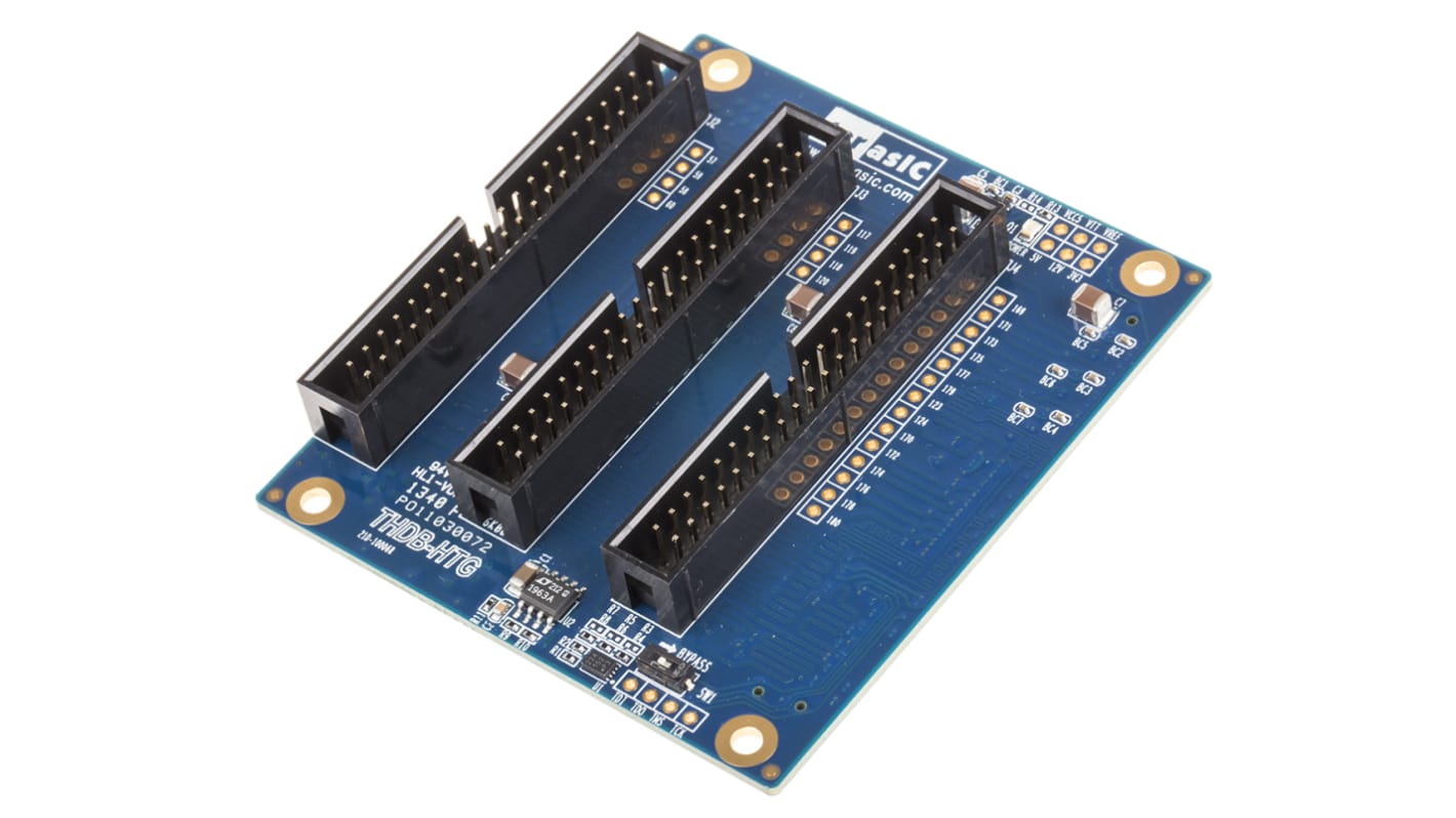
Terasic GPIO-HSTC Adapter Board
The HTG Card is designed to convert a High-Speed Terasic connector (HSTC) or a High-Speed Mezzanine connector (HSMC) I/Os to three 40-pin expansion prototype connectors, which are compatible with Altera DE3/DE2-115/DE2/DE1/DE0 expansion headers. Users can connect up to three Altera DE3/DE2-115/DE2/DE1/DE0 boards (or associated daughter cards) onto a HSTC/HSMC-interfaced host board via a HTG Card.
Convert HSTC/HSMC-interfaced I/O to standard 40-pin expansion connectors
Allow users to connect Altera DE3/DE2-115/DE2/DE1/DE0 boards to a HSTC/HSMC-interfaced host board
Provide test points for signal measurement
An FPGA is a semiconductor device consisting of a matrix of Configurable Logic Blocks (CLBs) connected through programmable interconnects. The user determines these interconnections by programming SRAM. A CLB can be simple (AND, OR gates, etc) or complex (a block of RAM). The FPGA allows changes to be made to a design even after the device is soldered into a PCB.
Related links
- Terasic SDI to HSMC SDI HSMC Board Adapter Board for Stratix IV GX FPGA Development Board P0039
- Terasic Cyclone IV Deo-Nano Starter Kit for Cyclone IV P0082
- FTDI Chip FT311 GPIO Board UMFT311GP Interface Development Tools for FT311D Development Module
- FTDI Chip FT311 GPIO Board UMFT311GP Interface Development Tools for FT311D Development Module UMFT311GP
- Digilent USRP B205mini-i AD9364 RFIC GPS Development Board for JTAG, GPIO 6 GHz 6002-410-021
- MikroElektronika Communication & Wireless Development Tool for Wireless Communication Systems In Smart Metering,
- MikroElektronika Communication & Wireless Development Tool for Applications Requiring Additional I/Os, Such As
- MikroElektronika Communication & Wireless Development Tool for Wearable Devices