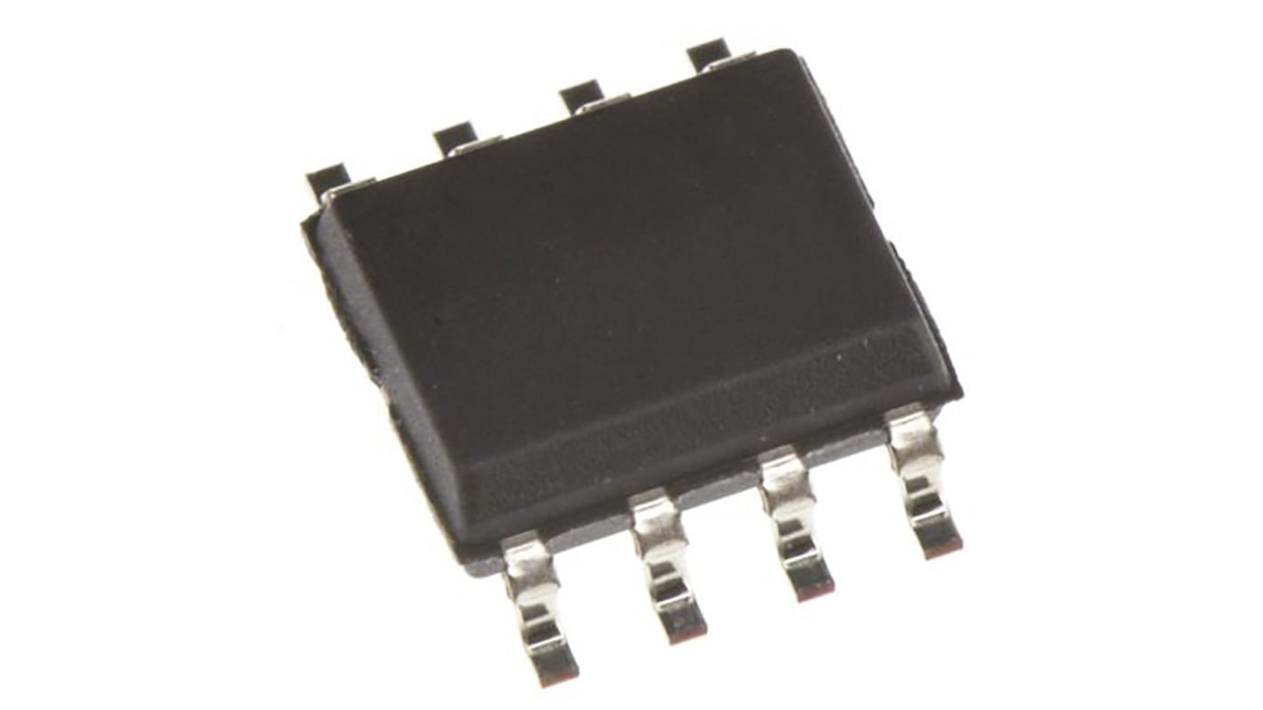
Infineon CY2305CSXI-1H PLL Clock Buffer 8-Pin SOIC
- RS Stock No.:
- 194-9009
- Mfr. Part No.:
- CY2305CSXI-1H
- Brand:
- Infineon

Stock information currently inaccessible
- RS Stock No.:
- 194-9009
- Mfr. Part No.:
- CY2305CSXI-1H
- Brand:
- Infineon
Specifications
Technical Reference
Legislation and Compliance
Product Details
Find similar products by selecting one or more attributes.
Select all | Attribute | Value |
|---|---|---|
| Brand | Infineon | |
| Number of Elements per Chip | 1 | |
| Maximum Supply Current | 35 mA | |
| Maximum Input Frequency | 133MHz | |
| Mounting Type | Surface Mount | |
| Package Type | SOIC | |
| Pin Count | 8 | |
| Dimensions | 4.97 x 3.98 x 1.47mm | |
| Length | 4.97mm | |
| Width | 3.98mm | |
| Height | 1.47mm | |
| Maximum Operating Supply Voltage | 3.6 V | |
| Maximum Operating Temperature | +85 °C | |
| Maximum Output Frequency | 133.33MHz | |
| Minimum Operating Supply Voltage | 3 V | |
| Minimum Output Frequency | 10MHz | |
| Minimum Operating Temperature | -40 °C | |
| Select all | ||
|---|---|---|
Brand Infineon | ||
Number of Elements per Chip 1 | ||
Maximum Supply Current 35 mA | ||
Maximum Input Frequency 133MHz | ||
Mounting Type Surface Mount | ||
Package Type SOIC | ||
Pin Count 8 | ||
Dimensions 4.97 x 3.98 x 1.47mm | ||
Length 4.97mm | ||
Width 3.98mm | ||
Height 1.47mm | ||
Maximum Operating Supply Voltage 3.6 V | ||
Maximum Operating Temperature +85 °C | ||
Maximum Output Frequency 133.33MHz | ||
Minimum Operating Supply Voltage 3 V | ||
Minimum Output Frequency 10MHz | ||
Minimum Operating Temperature -40 °C | ||
The CY2305C and CY2309C are die replacement parts for CY2305 and CY2309. The CY2309C is a low-cost 3.3 V zero delay buffer designed to distribute high speed clocks and is available in a 16-pin SOIC or TSSOP package. The CY2305C is an 8-pin version of the CY2309C. It accepts one reference input and drives out five low skew clocks. The -1H versions of each device operate up to 100 MHz–133 MHz frequencies and have higher drive than the -1 devices. All parts have on-chip phase locked loops (PLLs) which lock to an input clock on the REF pin. The PLL feedback is on-chip and is obtained from the CLKOUT pad. If all output clocks are not required, Bank B is three-stated. The input clock is directly applied to the outputs by the select inputs for chip and system testing purposes.
Related links
- Infineon CY2305CSXI-1H PLL Clock Buffer 8-Pin SOIC
- Infineon CY23EP05SXI-1H PLL Clock Buffer 8-Pin SOIC
- Infineon CY23EP05SXC-1H PLL Clock Buffer 8-Pin SOIC
- Infineon CY2308SXI-1H PLL Clock Buffer 16-Pin SOIC
- Infineon CY2309NZSXI-1H PLL Clock Buffer 16-Pin TSSOP
- Infineon CY23EP09ZXI-1H PLL Clock Buffer 16-Pin TSSOP
- Infineon CY2308ZXI-1H PLL Clock Buffer 16-Pin TSSOP
- Infineon CY2309NZSXC-1H PLL Clock Buffer 16-Pin TSSOP