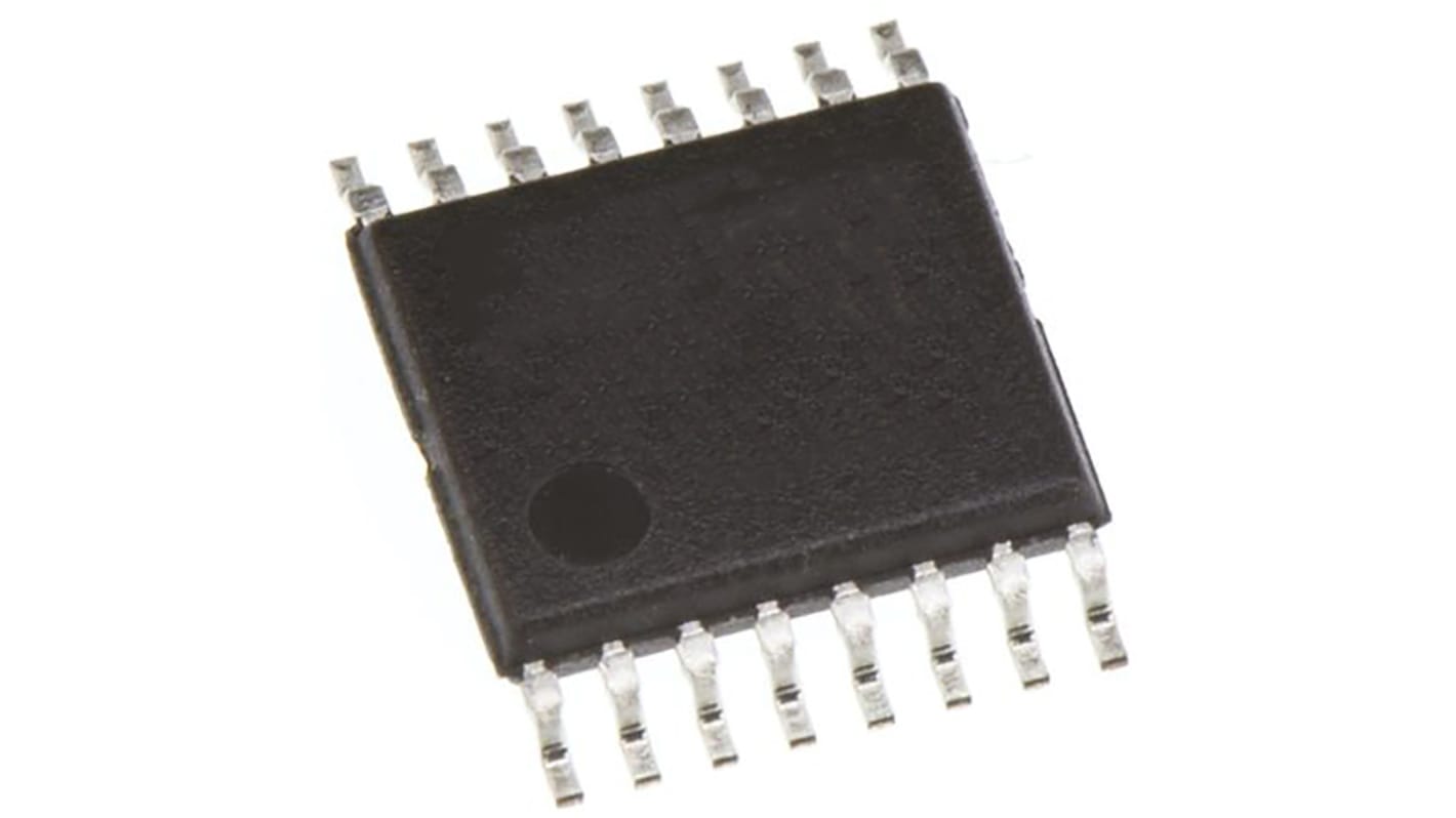
Infineon CY23EP09ZXI-1H PLL Clock Buffer 16-Pin TSSOP
- RS Stock No.:
- 194-9042
- Mfr. Part No.:
- CY23EP09ZXI-1H
- Brand:
- Infineon

Stock information currently inaccessible
- RS Stock No.:
- 194-9042
- Mfr. Part No.:
- CY23EP09ZXI-1H
- Brand:
- Infineon
Specifications
Technical Reference
Legislation and Compliance
Product Details
Find similar products by selecting one or more attributes.
Select all | Attribute | Value |
|---|---|---|
| Brand | Infineon | |
| Number of Elements per Chip | 1 | |
| Maximum Supply Current | 30 mA, 45 mA | |
| Maximum Input Frequency | 220MHz | |
| Mounting Type | Surface Mount | |
| Package Type | TSSOP | |
| Pin Count | 16 | |
| Dimensions | 5.1 x 4.5 x 0.95mm | |
| Length | 5.1mm | |
| Width | 4.5mm | |
| Height | 0.95mm | |
| Maximum Operating Supply Voltage | 3.6 V | |
| Maximum Operating Temperature | +85 °C | |
| Maximum Output Frequency | 220MHz | |
| Minimum Operating Supply Voltage | 3 V | |
| Minimum Operating Temperature | -40 °C | |
| Minimum Output Frequency | 10MHz | |
| Select all | ||
|---|---|---|
Brand Infineon | ||
Number of Elements per Chip 1 | ||
Maximum Supply Current 30 mA, 45 mA | ||
Maximum Input Frequency 220MHz | ||
Mounting Type Surface Mount | ||
Package Type TSSOP | ||
Pin Count 16 | ||
Dimensions 5.1 x 4.5 x 0.95mm | ||
Length 5.1mm | ||
Width 4.5mm | ||
Height 0.95mm | ||
Maximum Operating Supply Voltage 3.6 V | ||
Maximum Operating Temperature +85 °C | ||
Maximum Output Frequency 220MHz | ||
Minimum Operating Supply Voltage 3 V | ||
Minimum Operating Temperature -40 °C | ||
Minimum Output Frequency 10MHz | ||
The -1H version operates up to 220 (200) MHz frequencies at 3.3 V (2.5 V), and has higher drive than the -1 devices. All parts have on-chip PLLs that lock to an input clock on the REF pin. The phase-locked loop (PLL) feedback is on-chip and is obtained from the CLKOUT pad. There are two banks of four outputs each, which can be controlled by the Select inputs. If all output clocks are not required, Bank B can be three-stated. The select inputs also allow the input clock to be directly applied to the outputs for chip and system testing purposes. The PLL enters a power-down mode when there are no rising edges on the REF input (less than ∼2 MHz). In this state, the outputs are three-stated and the PLL is turned off, resulting in less than 25 μA of current draw. In the special case when S2:S1 is 1:0, the PLL is bypassed and REF is output from DC to the maximum allowable frequency. The part behaves like a non-zero delay buffer in this mode, and the outputs are not tri-stated.
Related links
- Infineon CY23EP09ZXI-1H PLL Clock Buffer 16-Pin TSSOP
- Infineon CY2308ZXI-1H PLL Clock Buffer 16-Pin TSSOP
- Infineon CY2309NZSXI-1H PLL Clock Buffer 16-Pin TSSOP
- Infineon CY2309SXI-1H PLL Clock Buffer 16-Pin TSSOP
- Infineon CY2309NZSXC-1H PLL Clock Buffer 16-Pin TSSOP
- Infineon CY2308SXI-1H PLL Clock Buffer 16-Pin SOIC
- Infineon CY22392FXC PLL Clock Buffer 16-Pin TSSOP
- Infineon CY2309SXC-1 PLL Clock Buffer 16-Pin TSSOP