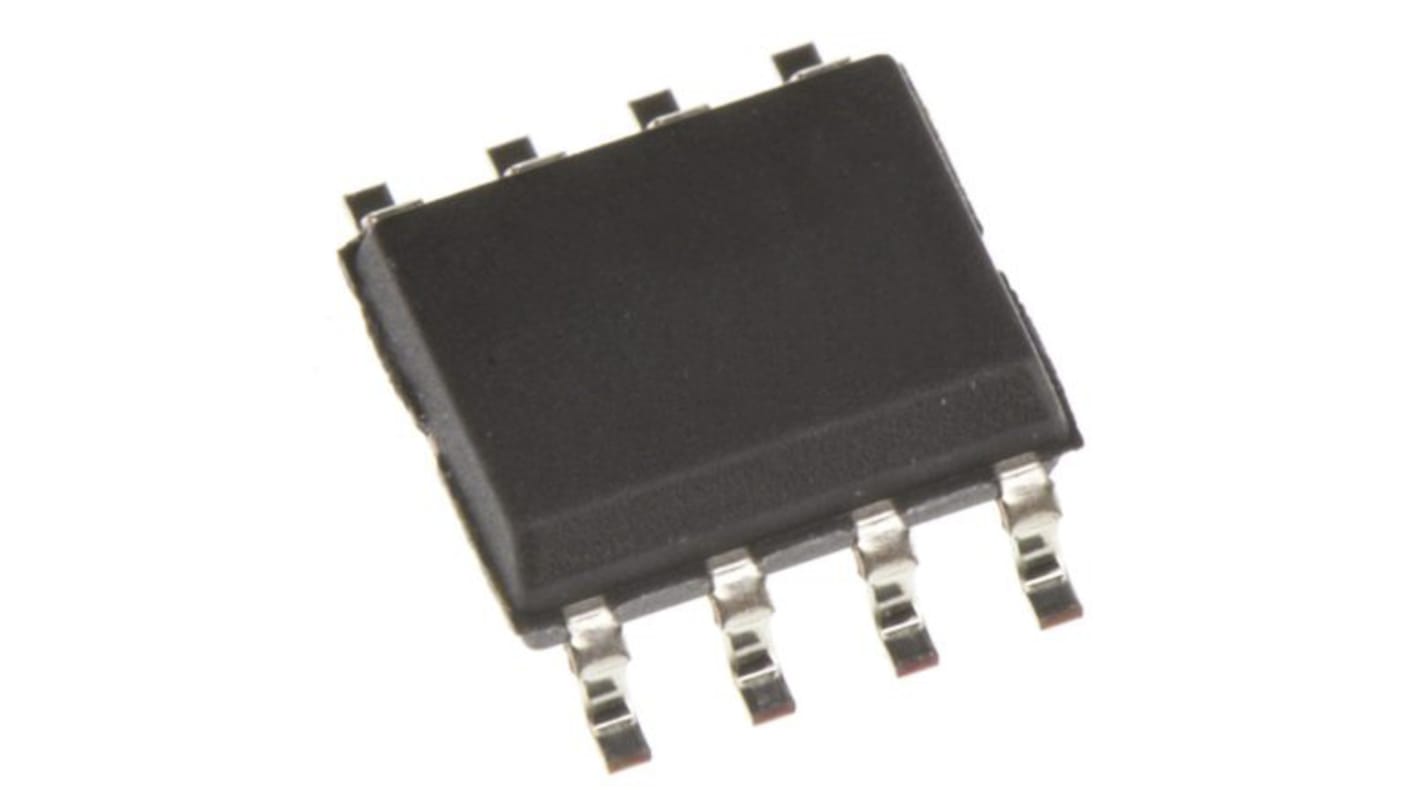
onsemi, Logic Level Translator Translator 2 ECL to LVTTL, 8-Pin SOIC
- RS Stock No.:
- 186-8831
- Mfr. Part No.:
- MC100EPT25DG
- Brand:
- onsemi

Subtotal (1 tube of 98 units)*
£521.85
(exc. VAT)
£626.22
(inc. VAT)
FREE delivery for orders over £60.00
- 1,666 unit(s) ready to ship
Units | Per unit | Per Tube* |
|---|---|---|
| 98 + | £5.325 | £521.85 |
*price indicative
- RS Stock No.:
- 186-8831
- Mfr. Part No.:
- MC100EPT25DG
- Brand:
- onsemi
Select all | Attribute | Value |
|---|---|---|
| Brand | onsemi | |
| Direction Type | Uni-Directional | |
| Logic Family | ECL | |
| Product Type | Logic Level Translator | |
| Maximum Propagation Delay Time @ CL | 2ns | |
| Mount Type | Surface | |
| Number of Elements per Chip | 2 | |
| Package Type | SOIC | |
| Pin Count | 8 | |
| Output Type | LVTTL | |
| Logic Function | Translator | |
| Maximum Low Level Output Current | 24mA | |
| Maximum High Level Output Current | -3mA | |
| Minimum Supply Voltage | 3V | |
| Translation | ECL to LVTTL | |
| Maximum Supply Voltage | 3.6V | |
| Minimum Operating Temperature | -40°C | |
| Maximum Operating Temperature | 85°C | |
| Height | 1.5mm | |
| Series | MC100EPT2 | |
| Standards/Approvals | No | |
| Length | 5mm | |
| Automotive Standard | No | |
| Select all | ||
|---|---|---|
Brand onsemi | ||
Direction Type Uni-Directional | ||
Logic Family ECL | ||
Product Type Logic Level Translator | ||
Maximum Propagation Delay Time @ CL 2ns | ||
Mount Type Surface | ||
Number of Elements per Chip 2 | ||
Package Type SOIC | ||
Pin Count 8 | ||
Output Type LVTTL | ||
Logic Function Translator | ||
Maximum Low Level Output Current 24mA | ||
Maximum High Level Output Current -3mA | ||
Minimum Supply Voltage 3V | ||
Translation ECL to LVTTL | ||
Maximum Supply Voltage 3.6V | ||
Minimum Operating Temperature -40°C | ||
Maximum Operating Temperature 85°C | ||
Height 1.5mm | ||
Series MC100EPT2 | ||
Standards/Approvals No | ||
Length 5mm | ||
Automotive Standard No | ||
