onsemi, Voltage Level Shifter Buffer 2 CMOS, 20-Pin TSSOP
- RS Stock No.:
- 186-8366P
- Mfr. Part No.:
- 74LCX244MTC
- Brand:
- onsemi

Subtotal 25 units (supplied in a tube)*
£7.025
(exc. VAT)
£8.425
(inc. VAT)
FREE delivery for orders over £60.00
In Stock
- Plus 1,250 unit(s) shipping from 08 June 2026
Need more? Click ‘Check delivery dates’ to find extra stock and lead times.
Units | Per unit |
|---|---|
| 25 + | £0.281 |
*price indicative
- RS Stock No.:
- 186-8366P
- Mfr. Part No.:
- 74LCX244MTC
- Brand:
- onsemi
Specifications
Technical Reference
Legislation and Compliance
Product Details
Find similar products by selecting one or more attributes.
Select all | Attribute | Value |
|---|---|---|
| Brand | onsemi | |
| Direction Type | Bi-Directional | |
| Product Type | Voltage Level Shifter | |
| Logic Family | LCX | |
| Maximum Propagation Delay Time @ CL | 9ns | |
| Mount Type | Surface | |
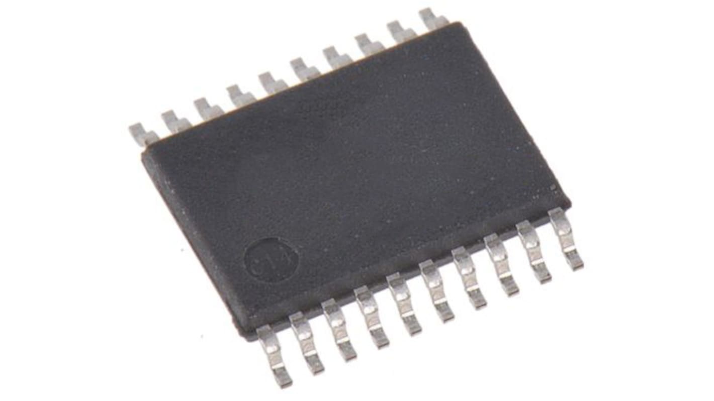
| Package Type | TSSOP | |
| Number of Elements per Chip | 2 | |
| Pin Count | 20 | |
| Output Type | 3 State | |
| Logic Function | Buffer | |
| Maximum Low Level Output Current | 24mA | |
| Minimum Supply Voltage | 2V | |
| Maximum High Level Output Current | -24mA | |
| Maximum Supply Voltage | 3.6V | |
| Translation | CMOS | |
| Minimum Operating Temperature | -40°C | |
| Maximum Operating Temperature | 85°C | |
| Length | 6.6mm | |
| Height | 1.05mm | |
| Standards/Approvals | No | |
| Series | 74LCX244 | |
| Automotive Standard | No | |
| Select all | ||
|---|---|---|
Brand onsemi | ||
Direction Type Bi-Directional | ||
Product Type Voltage Level Shifter | ||
Logic Family LCX | ||
Maximum Propagation Delay Time @ CL 9ns | ||
Mount Type Surface | ||
Package Type TSSOP | ||
Number of Elements per Chip 2 | ||
Pin Count 20 | ||
Output Type 3 State | ||
Logic Function Buffer | ||
Maximum Low Level Output Current 24mA | ||
Minimum Supply Voltage 2V | ||
Maximum High Level Output Current -24mA | ||
Maximum Supply Voltage 3.6V | ||
Translation CMOS | ||
Minimum Operating Temperature -40°C | ||
Maximum Operating Temperature 85°C | ||
Length 6.6mm | ||
Height 1.05mm | ||
Standards/Approvals No | ||
Series 74LCX244 | ||
Automotive Standard No | ||
The LCX244 contains eight non-inverting buffers with 3-STATE outputs. The device may be employed as a memory address driver, clock driver and bus-oriented transmitter/receiver. The LCX244 is designed for low voltage (2.5V or 3.3V) VCC applications with capability of interfacing to a 5V signal environment. The LCX244 is fabricated with an advanced CMOS technology to achieve high speed operation while maintaining CMOS low power dissipation.
5V tolerant inputs and outputs
2.3V to 3.6V VCC specifications provided
6.5 ns tPD max (VCC = 3.3V), 10 μA ICC max
Power down high impedance inputs and outputs
Supports live insertion/withdrawal (Note 1)
±24 mA output drive (VCC = 3.0V)
Implements patented noise/EMI reduction circuitry
Latch-up performance exceeds 500 mA
ESD performance: Human body model > 2000V Machine model > 200V
Leadless DQFN Pb-Free package
Applications
This product is general usage and suitable for many different applications.