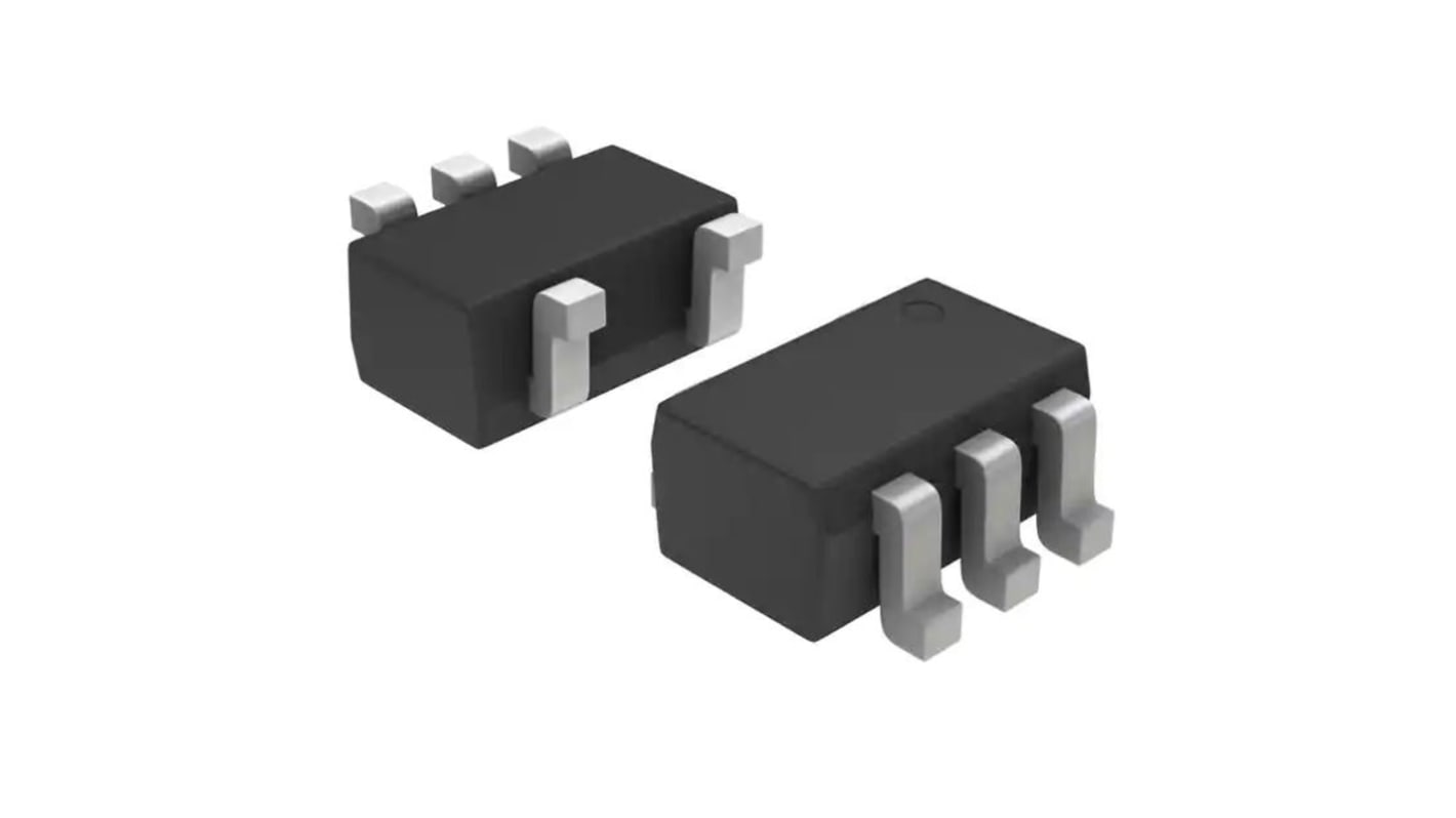
onsemi M74VHC1GT126DF2G, Voltage Level Shifter Buffer 1, 5-Pin SC
- RS Stock No.:
- 186-8304
- Mfr. Part No.:
- M74VHC1GT126DF2G
- Brand:
- onsemi

Stock information currently inaccessible
- RS Stock No.:
- 186-8304
- Mfr. Part No.:
- M74VHC1GT126DF2G
- Brand:
- onsemi
Specifications
Technical Reference
Legislation and Compliance
Product Details
Find similar products by selecting one or more attributes.
Select all | Attribute | Value |
|---|---|---|
| Brand | onsemi | |
| Logic Family | VHC | |
| Mounting Type | Surface Mount | |
| Package Type | SC | |
| Number of Elements per Chip | 1 | |
| Pin Count | 5 | |
| Output Type | 3 State | |
| Dimensions | 2.2 x 1.35 x 1mm | |
| Logic Function | Buffer | |
| Maximum Low Level Output Current | 8mA | |
| Maximum High Level Output Current | -8mA | |
| Propagation Delay Test Condition | 50pF | |
| Maximum Propagation Delay Time @ Maximum CL | 16 ns @ 50 pF | |
| Maximum Operating Supply Voltage | 2 to 5.5 V | |
| Maximum Operating Temperature | +125 °C | |
| Minimum Operating Supply Voltage | 2 V | |
| Minimum Operating Temperature | -55 °C | |
| Automotive Standard | AEC-Q100 | |
| Select all | ||
|---|---|---|
Brand onsemi | ||
Logic Family VHC | ||
Mounting Type Surface Mount | ||
Package Type SC | ||
Number of Elements per Chip 1 | ||
Pin Count 5 | ||
Output Type 3 State | ||
Dimensions 2.2 x 1.35 x 1mm | ||
Logic Function Buffer | ||
Maximum Low Level Output Current 8mA | ||
Maximum High Level Output Current -8mA | ||
Propagation Delay Test Condition 50pF | ||
Maximum Propagation Delay Time @ Maximum CL 16 ns @ 50 pF | ||
Maximum Operating Supply Voltage 2 to 5.5 V | ||
Maximum Operating Temperature +125 °C | ||
Minimum Operating Supply Voltage 2 V | ||
Minimum Operating Temperature -55 °C | ||
Automotive Standard AEC-Q100 | ||
High Speed: tPD = 3.5ns (Typ) at V CC = 5V
Low Power Dissipation: ICC = 1μA (Max) at TA = 25°C
TTL-Compatible Inputs: VIL = 0.8V, VIH = 2.0V
CMOS-Compatible Outputs: VOH > 0.8VCC , VOL < 0.1VCC @Load
Power Down Protection Provided on Inputs and Outputs
Balanced Propagation Delays
Pin and Function Compatible with Other Standard Logic Families
Chip Complexity: FETs = 62, Equivalent Gates = 16
Pb-Free Packages are Available