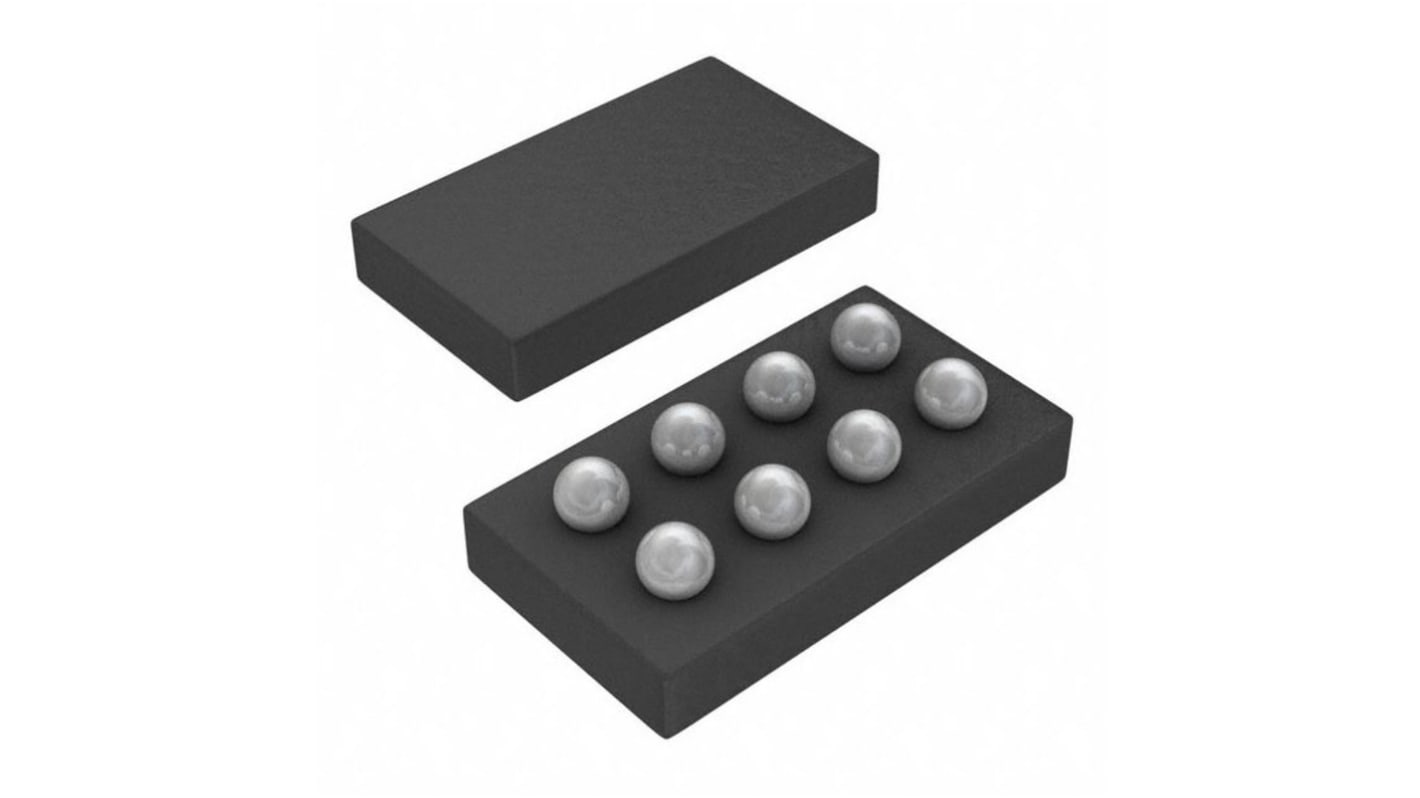
onsemi NLSX0102FC2T2G, Voltage Level Shifter Level Translator 2 Bi-Directional, 8-Pin Flip-Chip
- RS Stock No.:
- 185-8121
- Mfr. Part No.:
- NLSX0102FC2T2G
- Brand:
- onsemi

Stock information currently inaccessible
- RS Stock No.:
- 185-8121
- Mfr. Part No.:
- NLSX0102FC2T2G
- Brand:
- onsemi
Specifications
Technical Reference
Legislation and Compliance
Product Details
Find similar products by selecting one or more attributes.
Select all | Attribute | Value |
|---|---|---|
| Brand | onsemi | |
| Mounting Type | Surface Mount | |
| Number of Elements per Chip | 2 | |
| Package Type | Flip-Chip | |
| Pin Count | 8 | |
| Output Type | 3 State | |
| Logic Function | Level Translator | |
| Dimensions | 1.9 x 0.9 x 0.31mm | |
| Maximum Low Level Output Current | 1mA | |
| Maximum High Level Output Current | -20µA | |
| Translation | Bi-Directional | |
| Propagation Delay Test Condition | 15pF | |
| Maximum Operating Supply Voltage | 5.5 V | |
| Maximum Propagation Delay Time @ Maximum CL | 255 ns @ 15 pF | |
| Maximum Operating Temperature | +85 °C | |
| Minimum Operating Supply Voltage | 1.5 V | |
| Minimum Operating Temperature | -40 °C | |
| Select all | ||
|---|---|---|
Brand onsemi | ||
Mounting Type Surface Mount | ||
Number of Elements per Chip 2 | ||
Package Type Flip-Chip | ||
Pin Count 8 | ||
Output Type 3 State | ||
Logic Function Level Translator | ||
Dimensions 1.9 x 0.9 x 0.31mm | ||
Maximum Low Level Output Current 1mA | ||
Maximum High Level Output Current -20µA | ||
Translation Bi-Directional | ||
Propagation Delay Test Condition 15pF | ||
Maximum Operating Supply Voltage 5.5 V | ||
Maximum Propagation Delay Time @ Maximum CL 255 ns @ 15 pF | ||
Maximum Operating Temperature +85 °C | ||
Minimum Operating Supply Voltage 1.5 V | ||
Minimum Operating Temperature -40 °C | ||
- COO (Country of Origin):
- MY
VL can be Less than, Greater than or Equal to VCC
Wide VCC Operating Range: 1.5 V to 5.5 V
Wide VL Operating Range: 1.5 V to 5.5 V
High Speed with 24 Mb/s Guaranteed Date Rate
Low Bit to Bit Skew
Enable Input and I/O Pins are Overvoltage Tolerant (OVT) to 5.5 V
Non preferential Power up Sequencing
Integrated 10 k ohm Pull up Resistors
Small Space Saving Package:1.9 mm x 0.9 mm x 0.5 mm Flipchip8
This is a Pb Free Device
Low Voltage ASIC Level Translation
ESD Protection for All Pins: Human Body Model (HBM) > 7000 V
Applications
I2C, SMBus
End Products
Mobile Phones, PDAs, Cameras