Infineon SRAM Memory Chip, CY7C1049G30-10VXI- 4Mbit
- RS Stock No.:
- 193-8466
- Mfr. Part No.:
- CY7C1049G30-10VXI
- Brand:
- Infineon

Stock information currently inaccessible
- RS Stock No.:
- 193-8466
- Mfr. Part No.:
- CY7C1049G30-10VXI
- Brand:
- Infineon
Specifications
Technical Reference
Legislation and Compliance
Product Details
Find similar products by selecting one or more attributes.
Select all | Attribute | Value |
|---|---|---|
| Brand | Infineon | |
| Memory Size | 4Mbit | |
| Organisation | 512k x 8 bit | |
| Number of Words | 512k | |
| Number of Bits per Word | 8bit | |
| Maximum Random Access Time | 10ns | |
| Address Bus Width | 8bit | |
| Clock Frequency | 100MHz | |
| Timing Type | Asynchronous | |
| Mounting Type | Through Hole | |
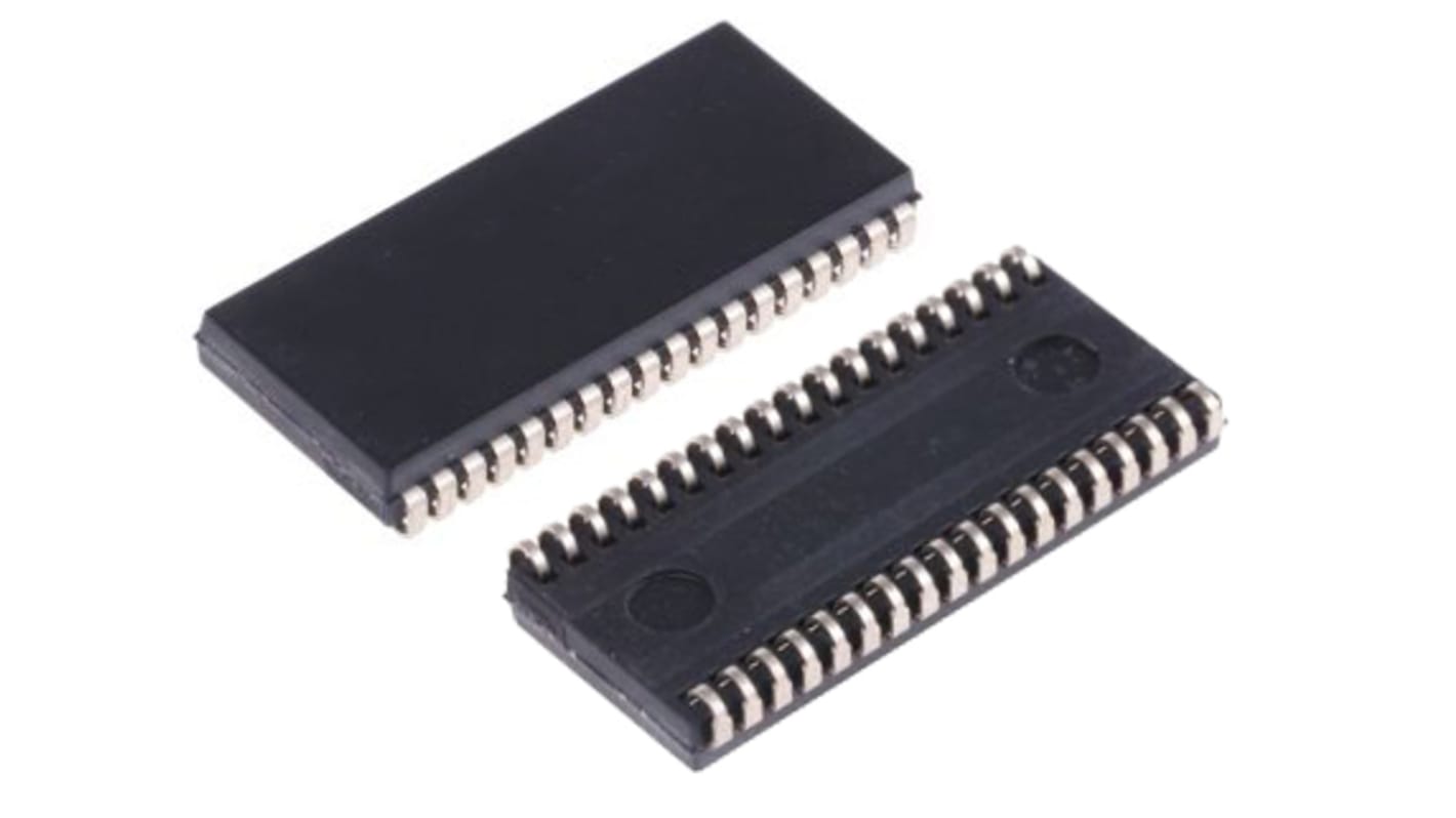
| Package Type | SOJ | |
| Pin Count | 36 | |
| Dimensions | 0.92 x 0.395 x 0.103in | |
| Maximum Operating Supply Voltage | 3.6 V | |
| Height | 2.62mm | |
| Width | 10.03mm | |
| Maximum Operating Temperature | +85 °C | |
| Length | 23.37mm | |
| Minimum Operating Supply Voltage | 2.2 V | |
| Minimum Operating Temperature | -40 °C | |
| Select all | ||
|---|---|---|
Brand Infineon | ||
Memory Size 4Mbit | ||
Organisation 512k x 8 bit | ||
Number of Words 512k | ||
Number of Bits per Word 8bit | ||
Maximum Random Access Time 10ns | ||
Address Bus Width 8bit | ||
Clock Frequency 100MHz | ||
Timing Type Asynchronous | ||
Mounting Type Through Hole | ||
Package Type SOJ | ||
Pin Count 36 | ||
Dimensions 0.92 x 0.395 x 0.103in | ||
Maximum Operating Supply Voltage 3.6 V | ||
Height 2.62mm | ||
Width 10.03mm | ||
Maximum Operating Temperature +85 °C | ||
Length 23.37mm | ||
Minimum Operating Supply Voltage 2.2 V | ||
Minimum Operating Temperature -40 °C | ||
CY7C1049G and CY7C1049GE are high-performance CMOS fast static RAM devices with embedded ECC. Both devices are offered in single and dual chip-enable options and in multiple pin configurations. The CY7C1049GE device includes an ERR pin that signals an error-detection and correction event during a read cycle. Data writes are performed by asserting the Chip Enable (CE) and Write Enable (WE) inputs LOW, while providing the data on I/O0through I/O7 and address on A0 through A18 pins. Data reads are performed by asserting the Chip Enable (CE) and Output Enable (OE) inputs LOW and providing the required address on the address lines. Read data is accessible on the I/O lines (I/O0 through I/O7).
High speed
tAA = 10 ns
Embedded ECC for single-bit error correction[1, 2]
Low active and standby currents
Active current: ICC = 38 mA typical
Standby current: ISB2 = 6 mA typical
Operating voltage range: 1.65 V to 2.2 V, 2.2 V to 3.6 V, and4.5 V to 5.5 V
1.0-V data retention
TTL-compatible inputs and outputs
Error indication (ERR) pin to indicate 1-bit error detection and correction
Pb-free 36-pin SOJ and 44-pin TSOP II packages