Dual N-Channel MOSFET, 111 A, 60 V, 8-Pin DFN onsemi NVMFD5C650NLT1G
- RS Stock No.:
- 172-3297
- Mfr. Part No.:
- NVMFD5C650NLT1G
- Brand:
- ON Semiconductor

Discontinued
- RS Stock No.:
- 172-3297
- Mfr. Part No.:
- NVMFD5C650NLT1G
- Brand:
- ON Semiconductor
Specifications
Technical Reference
Legislation and Compliance
Product Details
Find similar products by selecting one or more attributes.
Select all | Attribute | Value |
|---|---|---|
| Brand | ON Semiconductor | |
| Channel Type | N | |
| Maximum Continuous Drain Current | 111 A | |
| Maximum Drain Source Voltage | 60 V | |
| Package Type | DFN | |
| Mounting Type | Surface Mount | |
| Pin Count | 8 | |
| Maximum Drain Source Resistance | 5.8 mΩ | |
| Channel Mode | Enhancement | |
| Maximum Gate Threshold Voltage | 2.2V | |
| Minimum Gate Threshold Voltage | 1.2V | |
| Maximum Power Dissipation | 125 W | |
| Maximum Gate Source Voltage | ±20 V | |
| Typical Gate Charge @ Vgs | 37 nC @ 10 V | |
| Number of Elements per Chip | 2 | |
| Width | 5.1mm | |
| Maximum Operating Temperature | +175 °C | |
| Length | 6.1mm | |
| Automotive Standard | AEC-Q101 | |
| Height | 1.05mm | |
| Forward Diode Voltage | 1.2V | |
| Minimum Operating Temperature | -55 °C | |
| Series | NVMFD5C650NL | |
| Select all | ||
|---|---|---|
Brand ON Semiconductor | ||
Channel Type N | ||
Maximum Continuous Drain Current 111 A | ||
Maximum Drain Source Voltage 60 V | ||
Package Type DFN | ||
Mounting Type Surface Mount | ||
Pin Count 8 | ||
Maximum Drain Source Resistance 5.8 mΩ | ||
Channel Mode Enhancement | ||
Maximum Gate Threshold Voltage 2.2V | ||
Minimum Gate Threshold Voltage 1.2V | ||
Maximum Power Dissipation 125 W | ||
Maximum Gate Source Voltage ±20 V | ||
Typical Gate Charge @ Vgs 37 nC @ 10 V | ||
Number of Elements per Chip 2 | ||
Width 5.1mm | ||
Maximum Operating Temperature +175 °C | ||
Length 6.1mm | ||
Automotive Standard AEC-Q101 | ||
Height 1.05mm | ||
Forward Diode Voltage 1.2V | ||
Minimum Operating Temperature -55 °C | ||
Series NVMFD5C650NL | ||
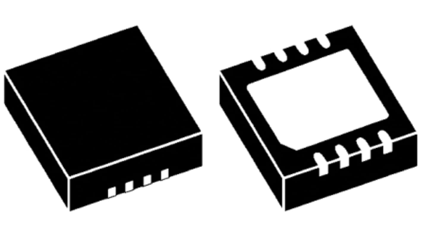
Automotive Power MOSFET in a 5x6mm flat lead package designed for compact and efficient designs and including high thermal performance. Wettable Flank Option available for Enhanced Optical Inspection. MOSFET and PPAP capable suitable for automotive applications.
Small Footprint (5x6 mm)
Compact Design
Low rDS(on)
Minimize Conduction Loss
Low QG and Capacitance
Minimize Driver Losses
NVMFD5C446NLWF − Wettable Flank Option
Enhanced Optical Inspection
PPAP Capable
Applications
Solenoid driver
Low side / high side driver
Automotive engine controllers
Antilock braking systems
Compact Design
Low rDS(on)
Minimize Conduction Loss
Low QG and Capacitance
Minimize Driver Losses
NVMFD5C446NLWF − Wettable Flank Option
Enhanced Optical Inspection
PPAP Capable
Applications
Solenoid driver
Low side / high side driver
Automotive engine controllers
Antilock braking systems