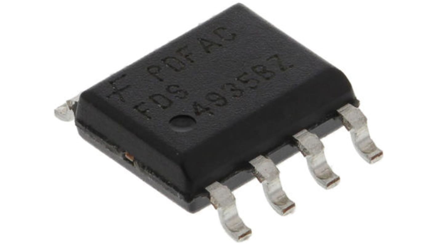
onsemi PowerTrench Dual N/P-Channel MOSFET, 3.5 A, 4.5 A, 60 V, 8-Pin SOIC FDS4559
- RS Stock No.:
- 917-5471P
- Mfr. Part No.:
- FDS4559
- Brand:
- onsemi

Bulk discount available
Subtotal 100 units (supplied on a continuous strip)*
£54.40
(exc. VAT)
£65.30
(inc. VAT)
FREE delivery for orders over £50.00
Temporarily out of stock
- 6,170 unit(s) shipping from 04 November 2025
Need more? Click ‘Check delivery dates’ to find extra stock and lead times.
Units | Per unit |
|---|---|
| 100 - 240 | £0.544 |
| 250 - 490 | £0.472 |
| 500 - 990 | £0.415 |
| 1000 + | £0.377 |
*price indicative
- RS Stock No.:
- 917-5471P
- Mfr. Part No.:
- FDS4559
- Brand:
- onsemi
Specifications
Technical Reference
Legislation and Compliance
Product Details
Find similar products by selecting one or more attributes.
Select all | Attribute | Value |
|---|---|---|
| Brand | onsemi | |
| Channel Type | N, P | |
| Maximum Continuous Drain Current | 3.5 A, 4.5 A | |
| Maximum Drain Source Voltage | 60 V | |
| Series | PowerTrench | |
| Package Type | SOIC | |
| Mounting Type | Surface Mount | |
| Pin Count | 8 | |
| Maximum Drain Source Resistance | 55 mΩ, 105 mΩ | |
| Channel Mode | Enhancement | |
| Maximum Power Dissipation | 2 W | |
| Transistor Configuration | Isolated | |
| Maximum Gate Source Voltage | -20 V, +20 V | |
| Width | 4mm | |
| Typical Gate Charge @ Vgs | 12.5 nC @ 10 V, 15 nC @ 10 V | |
| Number of Elements per Chip | 2 | |
| Maximum Operating Temperature | +175 °C | |
| Length | 5mm | |
| Transistor Material | Si | |
| Minimum Operating Temperature | -55 °C | |
| Height | 1.5mm | |
| Select all | ||
|---|---|---|
Brand onsemi | ||
Channel Type N, P | ||
Maximum Continuous Drain Current 3.5 A, 4.5 A | ||
Maximum Drain Source Voltage 60 V | ||
Series PowerTrench | ||
Package Type SOIC | ||
Mounting Type Surface Mount | ||
Pin Count 8 | ||
Maximum Drain Source Resistance 55 mΩ, 105 mΩ | ||
Channel Mode Enhancement | ||
Maximum Power Dissipation 2 W | ||
Transistor Configuration Isolated | ||
Maximum Gate Source Voltage -20 V, +20 V | ||
Width 4mm | ||
Typical Gate Charge @ Vgs 12.5 nC @ 10 V, 15 nC @ 10 V | ||
Number of Elements per Chip 2 | ||
Maximum Operating Temperature +175 °C | ||
Length 5mm | ||
Transistor Material Si | ||
Minimum Operating Temperature -55 °C | ||
Height 1.5mm | ||
PowerTrench® Dual N/P-Channel MOSFET, Fairchild Semiconductor
PowerTrench® MOSFETs are optimised power switches that offer increase of system efficiency and power density. They combine small gate charge(Qg), small reverse recovery charge(Qrr) and soft reverse recovery body diode, which contributes to fast switching of synchronous rectification in AC/DC power supplies.
The latest PowerTrench® MOSFETs, employ shielded-gate structure that provides charge balance. By utilizing this advanced technology, the FOM (Figure of Merit) of these devices is significant lower than that of previous generation.
Soft body diode performance of the PowerTrench® MOSFETs is able to eliminate snubber circuit or replace a higher voltage rating MOSFET.
MOSFET Transistors, ON Semi
ON Semi offers a substantial portfolio of MOSFET devices that includes high-voltage (>250V) and low-voltage (<250V) types. The advanced silicon technology provides smaller die sizes, which it is incorporated into multiple industry-standard and thermally-enhanced packages.
ON Semi MOSFETs provide superior design reliability from reduced voltage spikes and overshoot, to lower junction capacitance and reverse recovery charge, to elimination of additional external components to keep systems up and running longer.
ON Semi MOSFETs provide superior design reliability from reduced voltage spikes and overshoot, to lower junction capacitance and reverse recovery charge, to elimination of additional external components to keep systems up and running longer.