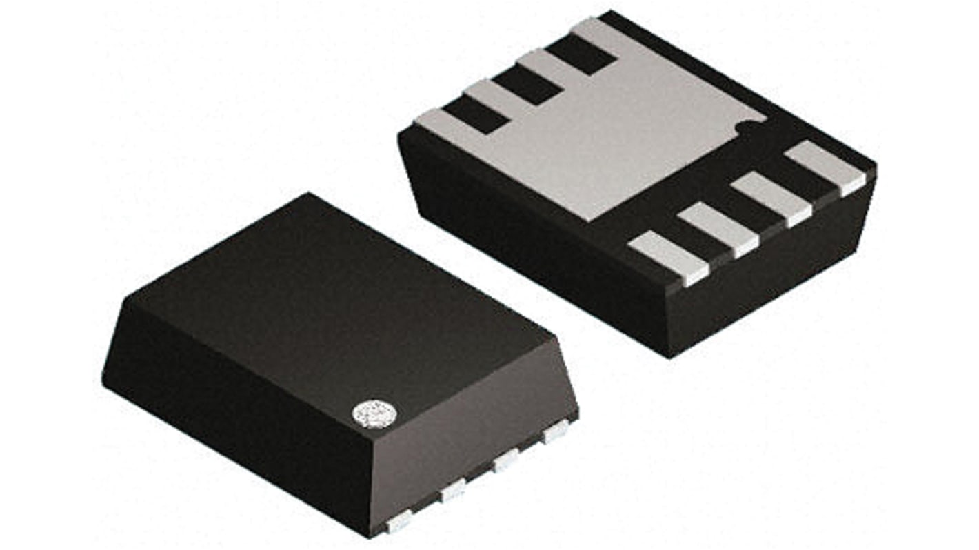
onsemi UltraFET N-Channel MOSFET, 27 A, 150 V, 8-Pin PQFN8 FDMS2572
- RS Stock No.:
- 864-4986
- Mfr. Part No.:
- FDMS2572
- Brand:
- onsemi

Subtotal (1 reel of 3000 units)*
£2,685.00
(exc. VAT)
£3,222.00
(inc. VAT)
FREE delivery for orders over £50.00
- 3,000 left, ready to ship
Units | Per unit | Per Reel* |
|---|---|---|
| 3000 + | £0.895 | £2,685.00 |
*price indicative
- RS Stock No.:
- 864-4986
- Mfr. Part No.:
- FDMS2572
- Brand:
- onsemi
Select all | Attribute | Value |
|---|---|---|
| Brand | onsemi | |
| Channel Type | N | |
| Maximum Continuous Drain Current | 27 A | |
| Maximum Drain Source Voltage | 150 V | |
| Series | UltraFET | |
| Package Type | PQFN8 | |
| Mounting Type | Surface Mount | |
| Pin Count | 8 | |
| Maximum Drain Source Resistance | 103 mΩ | |
| Channel Mode | Enhancement | |
| Minimum Gate Threshold Voltage | 2V | |
| Maximum Power Dissipation | 78 W | |
| Transistor Configuration | Single | |
| Maximum Gate Source Voltage | -20 V, +20 V | |
| Width | 6mm | |
| Maximum Operating Temperature | +150 °C | |
| Number of Elements per Chip | 1 | |
| Length | 5mm | |
| Transistor Material | Si | |
| Typical Gate Charge @ Vgs | 31 nC @ 10 V | |
| Minimum Operating Temperature | -55 °C | |
| Height | 0.75mm | |
Select all | ||
|---|---|---|
Brand onsemi | ||
Channel Type N | ||
Maximum Continuous Drain Current 27 A | ||
Maximum Drain Source Voltage 150 V | ||
Series UltraFET | ||
Package Type PQFN8 | ||
Mounting Type Surface Mount | ||
Pin Count 8 | ||
Maximum Drain Source Resistance 103 mΩ | ||
Channel Mode Enhancement | ||
Minimum Gate Threshold Voltage 2V | ||
Maximum Power Dissipation 78 W | ||
Transistor Configuration Single | ||
Maximum Gate Source Voltage -20 V, +20 V | ||
Width 6mm | ||
Maximum Operating Temperature +150 °C | ||
Number of Elements per Chip 1 | ||
Length 5mm | ||
Transistor Material Si | ||
Typical Gate Charge @ Vgs 31 nC @ 10 V | ||
Minimum Operating Temperature -55 °C | ||
Height 0.75mm | ||
UltraFET® MOSFET, Fairchild Semiconductor
Applications in high frequency DC to DC converters, switching regulators, motor drivers, low-voltage bus switches, and power management.
ON Semi MOSFETs provide superior design reliability from reduced voltage spikes and overshoot, to lower junction capacitance and reverse recovery charge, to elimination of additional external components to keep systems up and running longer.
