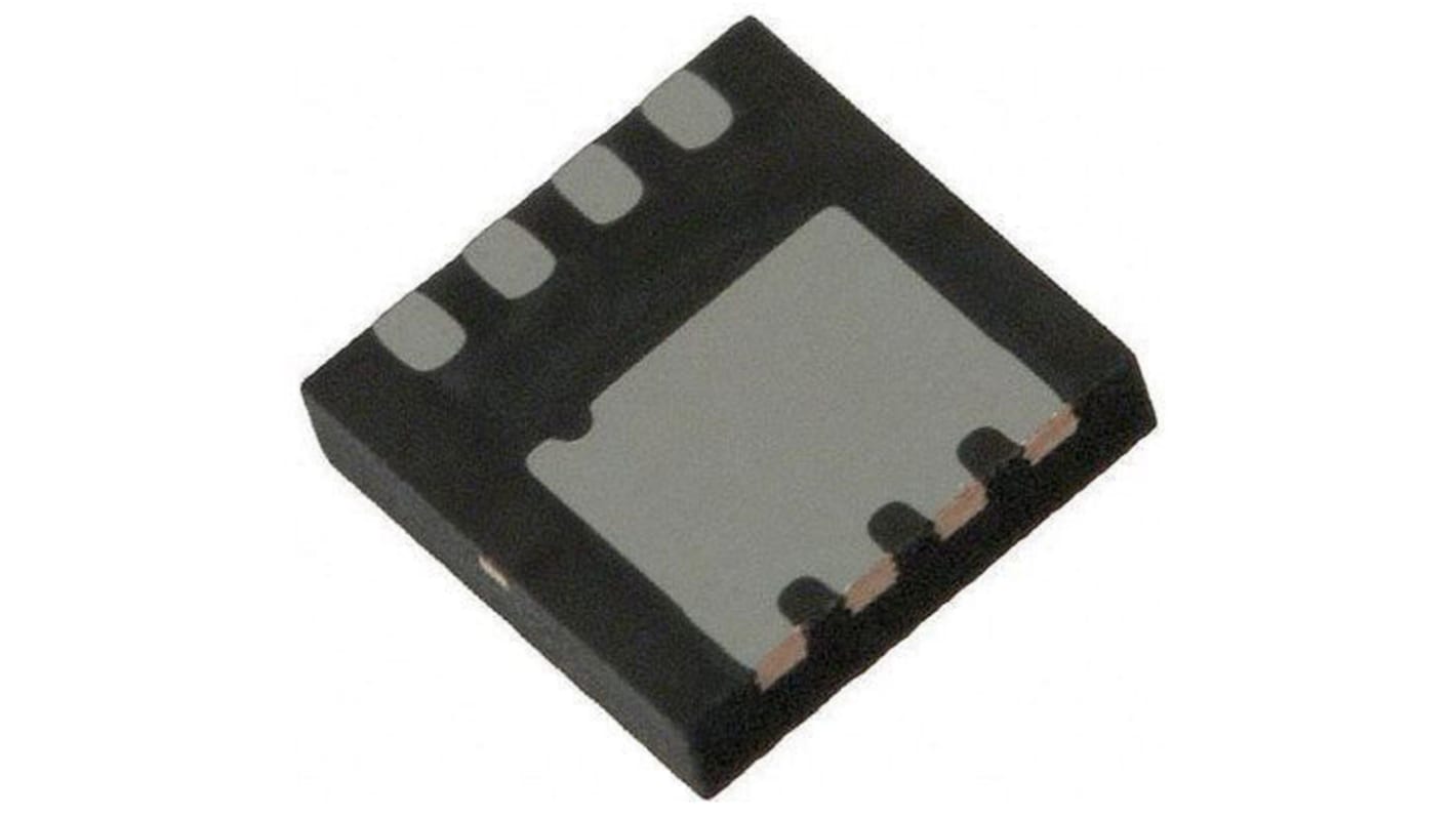
P-Channel MOSFET, 14 A, 60 V, 8-Pin MLP onsemi FDMC5614P
- RS Stock No.:
- 864-4869
- Mfr. Part No.:
- FDMC5614P
- Brand:
- ON Semiconductor

Stock information currently inaccessible
- RS Stock No.:
- 864-4869
- Mfr. Part No.:
- FDMC5614P
- Brand:
- ON Semiconductor
Specifications
Technical Reference
Legislation and Compliance
Find similar products by selecting one or more attributes.
Select all | Attribute | Value |
|---|---|---|
| Brand | ON Semiconductor | |
| Channel Type | P | |
| Maximum Continuous Drain Current | 14 A | |
| Maximum Drain Source Voltage | 60 V | |
| Package Type | MLP | |
| Mounting Type | Surface Mount | |
| Pin Count | 8 | |
| Maximum Drain Source Resistance | 168 mΩ | |
| Channel Mode | Enhancement | |
| Minimum Gate Threshold Voltage | 1V | |
| Maximum Power Dissipation | 42 W | |
| Transistor Configuration | Single | |
| Maximum Gate Source Voltage | -20 V, +20 V | |
| Number of Elements per Chip | 1 | |
| Maximum Operating Temperature | +150 °C | |
| Length | 3.3mm | |
| Typical Gate Charge @ Vgs | 15 nC @ 10 V | |
| Width | 3.3mm | |
| Transistor Material | Si | |
| Minimum Operating Temperature | -55 °C | |
| Height | 0.725mm | |
| Series | PowerTrench | |
| Select all | ||
|---|---|---|
Brand ON Semiconductor | ||
Channel Type P | ||
Maximum Continuous Drain Current 14 A | ||
Maximum Drain Source Voltage 60 V | ||
Package Type MLP | ||
Mounting Type Surface Mount | ||
Pin Count 8 | ||
Maximum Drain Source Resistance 168 mΩ | ||
Channel Mode Enhancement | ||
Minimum Gate Threshold Voltage 1V | ||
Maximum Power Dissipation 42 W | ||
Transistor Configuration Single | ||
Maximum Gate Source Voltage -20 V, +20 V | ||
Number of Elements per Chip 1 | ||
Maximum Operating Temperature +150 °C | ||
Length 3.3mm | ||
Typical Gate Charge @ Vgs 15 nC @ 10 V | ||
Width 3.3mm | ||
Transistor Material Si | ||
Minimum Operating Temperature -55 °C | ||
Height 0.725mm | ||
Series PowerTrench | ||