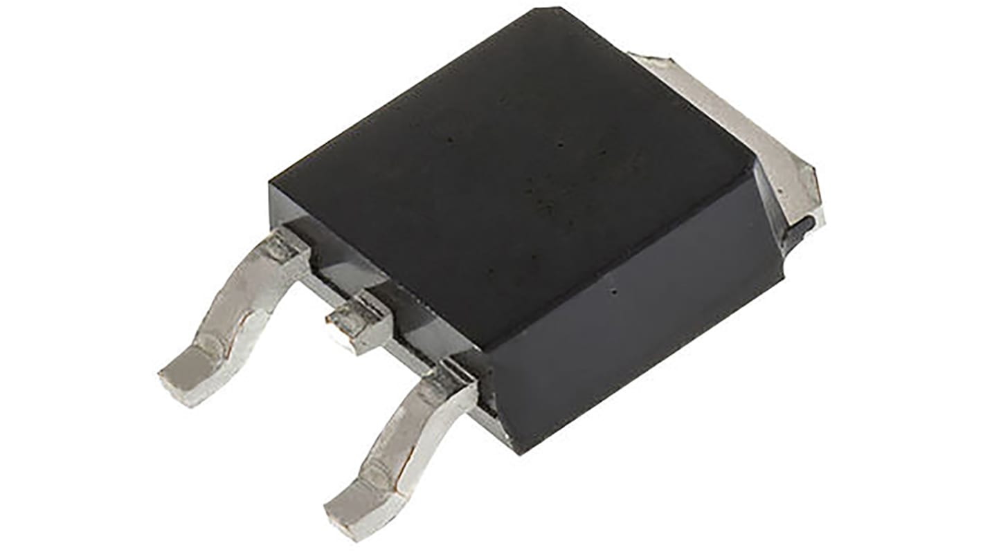
onsemi PowerTrench N-Channel MOSFET, 15.7 A, 100 V, 3-Pin DPAK FDD850N10L
- RS Stock No.:
- 809-0944P
- Mfr. Part No.:
- FDD850N10L
- Brand:
- onsemi

Subtotal 10 units (supplied on a continuous strip)*
£2.76
(exc. VAT)
£3.31
(inc. VAT)
FREE delivery for orders over £50.00
- Final 1,740 unit(s), ready to ship
Units | Per unit |
|---|---|
| 10 + | £0.276 |
*price indicative
- RS Stock No.:
- 809-0944P
- Mfr. Part No.:
- FDD850N10L
- Brand:
- onsemi
Select all | Attribute | Value |
|---|---|---|
| Brand | onsemi | |
| Channel Type | N | |
| Maximum Continuous Drain Current | 15.7 A | |
| Maximum Drain Source Voltage | 100 V | |
| Series | PowerTrench | |
| Package Type | DPAK (TO-252) | |
| Mounting Type | Surface Mount | |
| Pin Count | 3 | |
| Maximum Drain Source Resistance | 96 mΩ | |
| Channel Mode | Enhancement | |
| Minimum Gate Threshold Voltage | 1V | |
| Maximum Power Dissipation | 50 W | |
| Transistor Configuration | Single | |
| Maximum Gate Source Voltage | -20 V, +20 V | |
| Width | 6.22mm | |
| Transistor Material | Si | |
| Maximum Operating Temperature | +175 °C | |
| Length | 6.73mm | |
| Typical Gate Charge @ Vgs | 22.2 nC @ 10 V | |
| Number of Elements per Chip | 1 | |
| Height | 2.39mm | |
| Minimum Operating Temperature | -55 °C | |
| Select all | ||
|---|---|---|
Brand onsemi | ||
Channel Type N | ||
Maximum Continuous Drain Current 15.7 A | ||
Maximum Drain Source Voltage 100 V | ||
Series PowerTrench | ||
Package Type DPAK (TO-252) | ||
Mounting Type Surface Mount | ||
Pin Count 3 | ||
Maximum Drain Source Resistance 96 mΩ | ||
Channel Mode Enhancement | ||
Minimum Gate Threshold Voltage 1V | ||
Maximum Power Dissipation 50 W | ||
Transistor Configuration Single | ||
Maximum Gate Source Voltage -20 V, +20 V | ||
Width 6.22mm | ||
Transistor Material Si | ||
Maximum Operating Temperature +175 °C | ||
Length 6.73mm | ||
Typical Gate Charge @ Vgs 22.2 nC @ 10 V | ||
Number of Elements per Chip 1 | ||
Height 2.39mm | ||
Minimum Operating Temperature -55 °C | ||
PowerTrench® N-Channel MOSFET, 10A to 19.9A, Fairchild Semiconductor
ON Semi MOSFETs provide superior design reliability from reduced voltage spikes and overshoot, to lower junction capacitance and reverse recovery charge, to elimination of additional external components to keep systems up and running longer.
