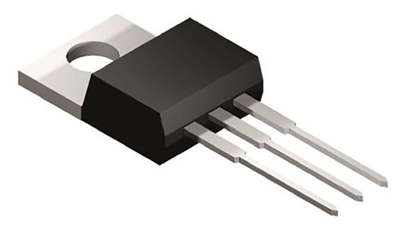
onsemi UltraFET N-Channel MOSFET, 75 A, 55 V, 3-Pin TO-220AB HUF75545P3
- RS Stock No.:
- 807-6695P
- Mfr. Part No.:
- HUF75545P3
- Brand:
- onsemi

Bulk discount available
Subtotal 20 units (supplied in a tube)*
£28.80
(exc. VAT)
£34.60
(inc. VAT)
FREE delivery for orders over £50.00
In Stock
- Plus 34 unit(s) shipping from 17 November 2025
Need more? Click ‘Check delivery dates’ to find extra stock and lead times.
Units | Per unit |
|---|---|
| 20 + | £1.44 |
*price indicative
- RS Stock No.:
- 807-6695P
- Mfr. Part No.:
- HUF75545P3
- Brand:
- onsemi
Specifications
Technical Reference
Legislation and Compliance
Product Details
Find similar products by selecting one or more attributes.
Select all | Attribute | Value |
|---|---|---|
| Brand | onsemi | |
| Channel Type | N | |
| Maximum Continuous Drain Current | 75 A | |
| Maximum Drain Source Voltage | 55 V | |
| Package Type | TO-220AB | |
| Series | UltraFET | |
| Mounting Type | Through Hole | |
| Pin Count | 3 | |
| Maximum Drain Source Resistance | 7 mΩ | |
| Channel Mode | Enhancement | |
| Minimum Gate Threshold Voltage | 2V | |
| Maximum Power Dissipation | 325 W | |
| Transistor Configuration | Single | |
| Maximum Gate Source Voltage | -20 V, +20 V | |
| Width | 4.7mm | |
| Length | 10.67mm | |
| Maximum Operating Temperature | +175 °C | |
| Number of Elements per Chip | 1 | |
| Typical Gate Charge @ Vgs | 220 nC @ 20 V | |
| Transistor Material | Si | |
| Height | 16.3mm | |
| Minimum Operating Temperature | -55 °C | |
| Select all | ||
|---|---|---|
Brand onsemi | ||
Channel Type N | ||
Maximum Continuous Drain Current 75 A | ||
Maximum Drain Source Voltage 55 V | ||
Package Type TO-220AB | ||
Series UltraFET | ||
Mounting Type Through Hole | ||
Pin Count 3 | ||
Maximum Drain Source Resistance 7 mΩ | ||
Channel Mode Enhancement | ||
Minimum Gate Threshold Voltage 2V | ||
Maximum Power Dissipation 325 W | ||
Transistor Configuration Single | ||
Maximum Gate Source Voltage -20 V, +20 V | ||
Width 4.7mm | ||
Length 10.67mm | ||
Maximum Operating Temperature +175 °C | ||
Number of Elements per Chip 1 | ||
Typical Gate Charge @ Vgs 220 nC @ 20 V | ||
Transistor Material Si | ||
Height 16.3mm | ||
Minimum Operating Temperature -55 °C | ||
UltraFET® MOSFET, Fairchild Semiconductor
UItraFET® Trench MOSFET combine characteristics that enable benchmark efficiency in power conversion applications. The device is capable of withstanding high energy in the avalanche mode, and the diode exhibits very low reverse recovery time and stored charge. Optimised for efficiency at high frequencies, lowest RDS(on), low ESR, and low total and Miller gate charge.
Applications in high frequency DC to DC converters, switching regulators, motor drivers, low-voltage bus switches, and power management.
Applications in high frequency DC to DC converters, switching regulators, motor drivers, low-voltage bus switches, and power management.
MOSFET Transistors, ON Semi
ON Semi offers a substantial portfolio of MOSFET devices that includes high-voltage (>250V) and low-voltage (<250V) types. The advanced silicon technology provides smaller die sizes, which it is incorporated into multiple industry-standard and thermally-enhanced packages.
ON Semi MOSFETs provide superior design reliability from reduced voltage spikes and overshoot, to lower junction capacitance and reverse recovery charge, to elimination of additional external components to keep systems up and running longer.
ON Semi MOSFETs provide superior design reliability from reduced voltage spikes and overshoot, to lower junction capacitance and reverse recovery charge, to elimination of additional external components to keep systems up and running longer.