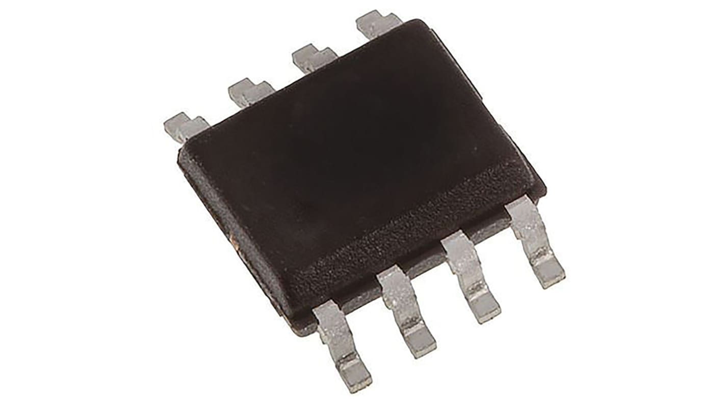
onsemi PowerTrench Dual N-Channel MOSFET, 4.5 A, 100 V, 8-Pin SOIC FDS3992
- RS Stock No.:
- 806-3649P
- Mfr. Part No.:
- FDS3992
- Brand:
- onsemi

Subtotal 25 units (supplied on a continuous strip)*
£33.80
(exc. VAT)
£40.55
(inc. VAT)
FREE delivery for orders over £50.00
- 1,735 unit(s) ready to ship
Units | Per unit |
|---|---|
| 25 - 120 | £1.352 |
| 125 - 620 | £1.326 |
| 625 - 1245 | £1.30 |
| 1250 + | £1.202 |
*price indicative
- RS Stock No.:
- 806-3649P
- Mfr. Part No.:
- FDS3992
- Brand:
- onsemi
Select all | Attribute | Value |
|---|---|---|
| Brand | onsemi | |
| Channel Type | N | |
| Maximum Continuous Drain Current | 4.5 A | |
| Maximum Drain Source Voltage | 100 V | |
| Package Type | SOIC | |
| Series | PowerTrench | |
| Mounting Type | Surface Mount | |
| Pin Count | 8 | |
| Maximum Drain Source Resistance | 123 mΩ | |
| Channel Mode | Enhancement | |
| Minimum Gate Threshold Voltage | 2V | |
| Maximum Power Dissipation | 2.5 W | |
| Transistor Configuration | Isolated | |
| Maximum Gate Source Voltage | -20 V, +20 V | |
| Maximum Operating Temperature | +150 °C | |
| Number of Elements per Chip | 2 | |
| Width | 3.9mm | |
| Typical Gate Charge @ Vgs | 11 nC @ 10 V | |
| Length | 4.9mm | |
| Transistor Material | Si | |
| Height | 1.575mm | |
| Minimum Operating Temperature | -55 °C | |
| Select all | ||
|---|---|---|
Brand onsemi | ||
Channel Type N | ||
Maximum Continuous Drain Current 4.5 A | ||
Maximum Drain Source Voltage 100 V | ||
Package Type SOIC | ||
Series PowerTrench | ||
Mounting Type Surface Mount | ||
Pin Count 8 | ||
Maximum Drain Source Resistance 123 mΩ | ||
Channel Mode Enhancement | ||
Minimum Gate Threshold Voltage 2V | ||
Maximum Power Dissipation 2.5 W | ||
Transistor Configuration Isolated | ||
Maximum Gate Source Voltage -20 V, +20 V | ||
Maximum Operating Temperature +150 °C | ||
Number of Elements per Chip 2 | ||
Width 3.9mm | ||
Typical Gate Charge @ Vgs 11 nC @ 10 V | ||
Length 4.9mm | ||
Transistor Material Si | ||
Height 1.575mm | ||
Minimum Operating Temperature -55 °C | ||
PowerTrench® Dual N-Channel MOSFET, Fairchild Semiconductor
The soft body diode performance of the PowerTrench® MOSFETs is able to eliminate snubber circuit or replace a higher voltage rating MOSFET.
ON Semi MOSFETs provide superior design reliability from reduced voltage spikes and overshoot, to lower junction capacitance and reverse recovery charge, to elimination of additional external components to keep systems up and running longer.
