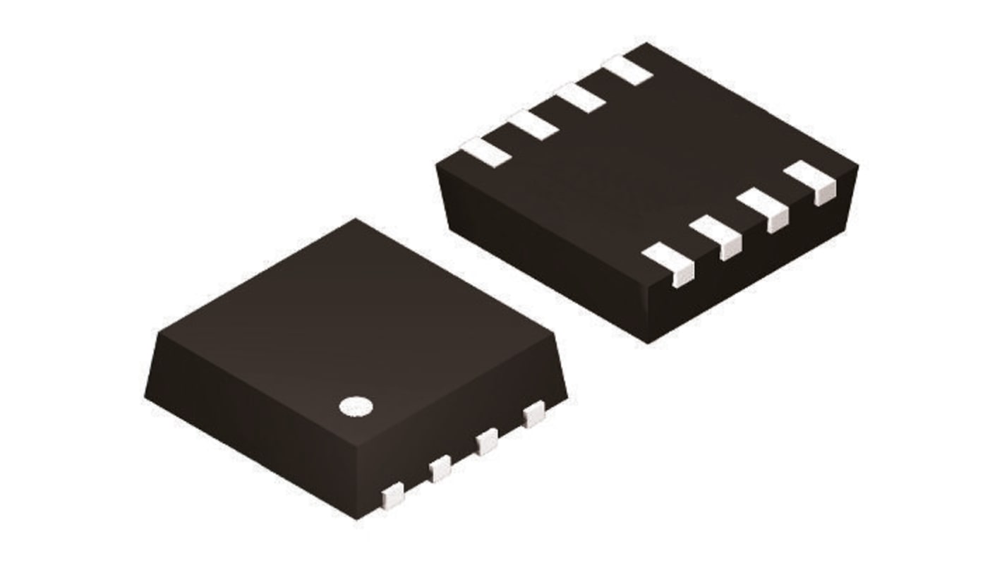
onsemi Dual N/P-Channel MOSFET, 5.5 A, 7 A, 30 V, 8-Pin ECH ECH8661-TL-H
- RS Stock No.:
- 802-0850P
- Mfr. Part No.:
- ECH8661-TL-H
- Brand:
- onsemi

Currently unavailable
Sorry, we don't know when this will be back in stock.
- RS Stock No.:
- 802-0850P
- Mfr. Part No.:
- ECH8661-TL-H
- Brand:
- onsemi
Specifications
Technical Reference
Legislation and Compliance
Product Details
Find similar products by selecting one or more attributes.
Select all | Attribute | Value |
|---|---|---|
| Brand | onsemi | |
| Channel Type | N, P | |
| Maximum Continuous Drain Current | 5.5 A, 7 A | |
| Maximum Drain Source Voltage | 30 V | |
| Package Type | ECH | |
| Mounting Type | Surface Mount | |
| Pin Count | 8 | |
| Maximum Drain Source Resistance | 24 mΩ, 39 mΩ | |
| Channel Mode | Enhancement | |
| Maximum Gate Threshold Voltage | 2.6V | |
| Maximum Power Dissipation | 1.3 W | |
| Transistor Configuration | Isolated | |
| Maximum Gate Source Voltage | -20 V, +20 V | |
| Number of Elements per Chip | 2 | |
| Length | 2.9mm | |
| Maximum Operating Temperature | +150 °C | |
| Width | 2.3mm | |
| Typical Gate Charge @ Vgs | 11.8 nC @ 10 V | |
| Transistor Material | Si | |
| Height | 0.9mm | |
| Select all | ||
|---|---|---|
Brand onsemi | ||
Channel Type N, P | ||
Maximum Continuous Drain Current 5.5 A, 7 A | ||
Maximum Drain Source Voltage 30 V | ||
Package Type ECH | ||
Mounting Type Surface Mount | ||
Pin Count 8 | ||
Maximum Drain Source Resistance 24 mΩ, 39 mΩ | ||
Channel Mode Enhancement | ||
Maximum Gate Threshold Voltage 2.6V | ||
Maximum Power Dissipation 1.3 W | ||
Transistor Configuration Isolated | ||
Maximum Gate Source Voltage -20 V, +20 V | ||
Number of Elements per Chip 2 | ||
Length 2.9mm | ||
Maximum Operating Temperature +150 °C | ||
Width 2.3mm | ||
Typical Gate Charge @ Vgs 11.8 nC @ 10 V | ||
Transistor Material Si | ||
Height 0.9mm | ||
Dual N/P-Channel MOSFET, ON Semiconductor
The NTJD1155L is a dual channel MOSFET. Featuring both P and N-channel’s into a single package, this MOSFET is brilliant for low control signal, low battery voltages and high load currents. The N-channel features internal ESD protection and can be driven by logic signals as low as 1.5V, while the P-Channel is designed to be used on load switching applications. The P-channel also designed with ON semi’s trench technology.
MOSFET Transistors, ON Semiconductor