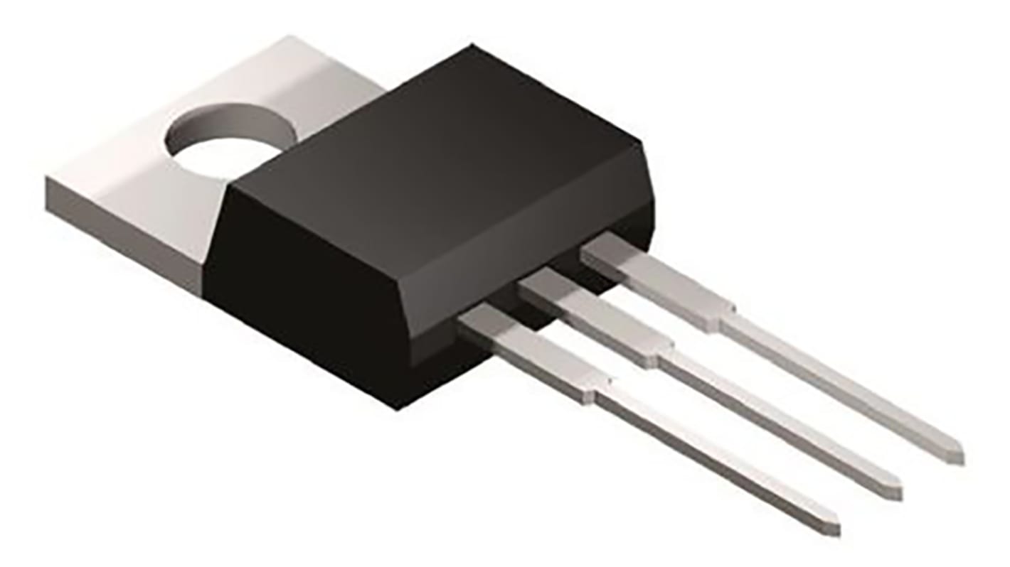
onsemi PowerTrench N-Channel MOSFET, 6 A, 100 V, 3-Pin TO-220AB FDP3682
- RS Stock No.:
- 671-4837
- Mfr. Part No.:
- FDP3682
- Brand:
- onsemi

Subtotal (1 pack of 5 units)*
£4.30
(exc. VAT)
£5.15
(inc. VAT)
FREE delivery for orders over £50.00
Temporarily out of stock
- Shipping from 12 January 2026
Need more? Click ‘Check delivery dates’ to find extra stock and lead times.
Units | Per unit | Per Pack* |
|---|---|---|
| 5 + | £0.86 | £4.30 |
*price indicative
- RS Stock No.:
- 671-4837
- Mfr. Part No.:
- FDP3682
- Brand:
- onsemi
Specifications
Technical Reference
Legislation and Compliance
Product Details
Find similar products by selecting one or more attributes.
Select all | Attribute | Value |
|---|---|---|
| Brand | onsemi | |
| Channel Type | N | |
| Maximum Continuous Drain Current | 6 A | |
| Maximum Drain Source Voltage | 100 V | |
| Series | PowerTrench | |
| Package Type | TO-220AB | |
| Mounting Type | Through Hole | |
| Pin Count | 3 | |
| Maximum Drain Source Resistance | 36 mΩ | |
| Channel Mode | Enhancement | |
| Minimum Gate Threshold Voltage | 2V | |
| Maximum Power Dissipation | 95 W | |
| Transistor Configuration | Single | |
| Maximum Gate Source Voltage | -20 V, +20 V | |
| Length | 10.67mm | |
| Number of Elements per Chip | 1 | |
| Width | 4.83mm | |
| Transistor Material | Si | |
| Maximum Operating Temperature | +175 °C | |
| Typical Gate Charge @ Vgs | 18.5 nC @ 10 V | |
| Minimum Operating Temperature | -55 °C | |
| Height | 9.4mm | |
Select all | ||
|---|---|---|
Brand onsemi | ||
Channel Type N | ||
Maximum Continuous Drain Current 6 A | ||
Maximum Drain Source Voltage 100 V | ||
Series PowerTrench | ||
Package Type TO-220AB | ||
Mounting Type Through Hole | ||
Pin Count 3 | ||
Maximum Drain Source Resistance 36 mΩ | ||
Channel Mode Enhancement | ||
Minimum Gate Threshold Voltage 2V | ||
Maximum Power Dissipation 95 W | ||
Transistor Configuration Single | ||
Maximum Gate Source Voltage -20 V, +20 V | ||
Length 10.67mm | ||
Number of Elements per Chip 1 | ||
Width 4.83mm | ||
Transistor Material Si | ||
Maximum Operating Temperature +175 °C | ||
Typical Gate Charge @ Vgs 18.5 nC @ 10 V | ||
Minimum Operating Temperature -55 °C | ||
Height 9.4mm | ||
PowerTrench® N-Channel MOSFET, up to 9.9A, Fairchild Semiconductor
MOSFET Transistors, ON Semi
ON Semi offers a substantial portfolio of MOSFET devices that includes high-voltage (>250V) and low-voltage (<250V) types. The advanced silicon technology provides smaller die sizes, which it is incorporated into multiple industry-standard and thermally-enhanced packages.
ON Semi MOSFETs provide superior design reliability from reduced voltage spikes and overshoot, to lower junction capacitance and reverse recovery charge, to elimination of additional external components to keep systems up and running longer.
ON Semi MOSFETs provide superior design reliability from reduced voltage spikes and overshoot, to lower junction capacitance and reverse recovery charge, to elimination of additional external components to keep systems up and running longer.