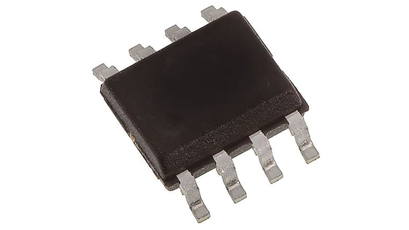
onsemi PowerTrench N-Channel MOSFET, 15 A, 30 V, 8-Pin SOIC FDS8896
- RS Stock No.:
- 671-0731
- Mfr. Part No.:
- FDS8896
- Brand:
- onsemi

Subtotal (1 pack of 5 units)*
£3.63
(exc. VAT)
£4.355
(inc. VAT)
Units | Per unit | Per Pack* |
|---|---|---|
| 5 - 45 | £0.726 | £3.63 |
| 50 - 95 | £0.626 | £3.13 |
| 100 - 495 | £0.542 | £2.71 |
| 500 - 995 | £0.476 | £2.38 |
| 1000 + | £0.434 | £2.17 |
*price indicative
- RS Stock No.:
- 671-0731
- Mfr. Part No.:
- FDS8896
- Brand:
- onsemi
Select all | Attribute | Value |
|---|---|---|
| Brand | onsemi | |
| Channel Type | N | |
| Maximum Continuous Drain Current | 15 A | |
| Maximum Drain Source Voltage | 30 V | |
| Series | PowerTrench | |
| Package Type | SOIC | |
| Mounting Type | Surface Mount | |
| Pin Count | 8 | |
| Maximum Drain Source Resistance | 6 mΩ | |
| Channel Mode | Enhancement | |
| Minimum Gate Threshold Voltage | 1.2V | |
| Maximum Power Dissipation | 2.5 W | |
| Transistor Configuration | Single | |
| Maximum Gate Source Voltage | -20 V, +20 V | |
| Maximum Operating Temperature | +150 °C | |
| Width | 4mm | |
| Length | 5mm | |
| Transistor Material | Si | |
| Number of Elements per Chip | 1 | |
| Typical Gate Charge @ Vgs | 50 nC @ 10 V | |
| Height | 1.5mm | |
| Minimum Operating Temperature | -55 °C | |
Select all | ||
|---|---|---|
Brand onsemi | ||
Channel Type N | ||
Maximum Continuous Drain Current 15 A | ||
Maximum Drain Source Voltage 30 V | ||
Series PowerTrench | ||
Package Type SOIC | ||
Mounting Type Surface Mount | ||
Pin Count 8 | ||
Maximum Drain Source Resistance 6 mΩ | ||
Channel Mode Enhancement | ||
Minimum Gate Threshold Voltage 1.2V | ||
Maximum Power Dissipation 2.5 W | ||
Transistor Configuration Single | ||
Maximum Gate Source Voltage -20 V, +20 V | ||
Maximum Operating Temperature +150 °C | ||
Width 4mm | ||
Length 5mm | ||
Transistor Material Si | ||
Number of Elements per Chip 1 | ||
Typical Gate Charge @ Vgs 50 nC @ 10 V | ||
Height 1.5mm | ||
Minimum Operating Temperature -55 °C | ||
PowerTrench® N-Channel MOSFET, 10A to 19.9A, Fairchild Semiconductor
ON Semi MOSFETs provide superior design reliability from reduced voltage spikes and overshoot, to lower junction capacitance and reverse recovery charge, to elimination of additional external components to keep systems up and running longer.
