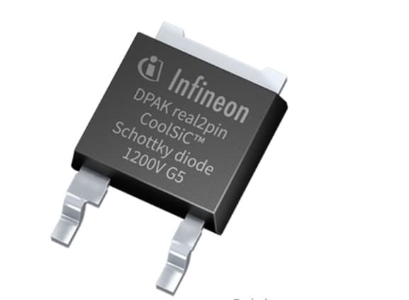
Infineon HEXFET P-Channel MOSFET, 70 A, 55 V, 3-Pin I2PAK IRF4905LPBF
- RS Stock No.:
- 650-3662P
- Mfr. Part No.:
- IRF4905LPBF
- Brand:
- Infineon

Subtotal 25 units (supplied in a tube)*
£28.10
(exc. VAT)
£33.725
(inc. VAT)
FREE delivery for orders over £50.00
- 5 unit(s) ready to ship
Units | Per unit |
|---|---|
| 25 - 45 | £1.124 |
| 50 - 120 | £1.054 |
| 125 - 245 | £0.986 |
| 250 + | £0.904 |
*price indicative
- RS Stock No.:
- 650-3662P
- Mfr. Part No.:
- IRF4905LPBF
- Brand:
- Infineon
Select all | Attribute | Value |
|---|---|---|
| Brand | Infineon | |
| Channel Type | P | |
| Maximum Continuous Drain Current | 70 A | |
| Maximum Drain Source Voltage | 55 V | |
| Package Type | I2PAK (TO-262) | |
| Series | HEXFET | |
| Mounting Type | Through Hole | |
| Pin Count | 3 | |
| Maximum Drain Source Resistance | 20 mΩ | |
| Channel Mode | Enhancement | |
| Maximum Gate Threshold Voltage | 4V | |
| Minimum Gate Threshold Voltage | 2V | |
| Maximum Power Dissipation | 3.8 W | |
| Transistor Configuration | Single | |
| Maximum Gate Source Voltage | -20 V, +20 V | |
| Transistor Material | Si | |
| Number of Elements per Chip | 1 | |
| Length | 10.67mm | |
| Maximum Operating Temperature | +175 °C | |
| Typical Gate Charge @ Vgs | 180 nC @ 10 V | |
| Width | 4.83mm | |
| Height | 10.54mm | |
| Minimum Operating Temperature | -55 °C | |
| Forward Diode Voltage | 1.3V | |
| Select all | ||
|---|---|---|
Brand Infineon | ||
Channel Type P | ||
Maximum Continuous Drain Current 70 A | ||
Maximum Drain Source Voltage 55 V | ||
Package Type I2PAK (TO-262) | ||
Series HEXFET | ||
Mounting Type Through Hole | ||
Pin Count 3 | ||
Maximum Drain Source Resistance 20 mΩ | ||
Channel Mode Enhancement | ||
Maximum Gate Threshold Voltage 4V | ||
Minimum Gate Threshold Voltage 2V | ||
Maximum Power Dissipation 3.8 W | ||
Transistor Configuration Single | ||
Maximum Gate Source Voltage -20 V, +20 V | ||
Transistor Material Si | ||
Number of Elements per Chip 1 | ||
Length 10.67mm | ||
Maximum Operating Temperature +175 °C | ||
Typical Gate Charge @ Vgs 180 nC @ 10 V | ||
Width 4.83mm | ||
Height 10.54mm | ||
Minimum Operating Temperature -55 °C | ||
Forward Diode Voltage 1.3V | ||
P-Channel Power MOSFET 40V to 55V, Infineon
Infineon HEXFET Series MOSFET, -70A Maximum Continuous Drain Current, 3.8W Maximum Power Dissipation - IRF4905LPBF
Features & Benefits
• Low RDS(on) for decreased power losses during operation
• Fast switching capabilities to improve efficiency
• Tolerates repetitive avalanche conditions without failure
• Effective gate charge characteristics for better circuit responsiveness
Applications
• Ideal for brushless DC motor control
• Applicable in automotive electronics for increased reliability
• Suitable for industrial automation systems that require robust components


