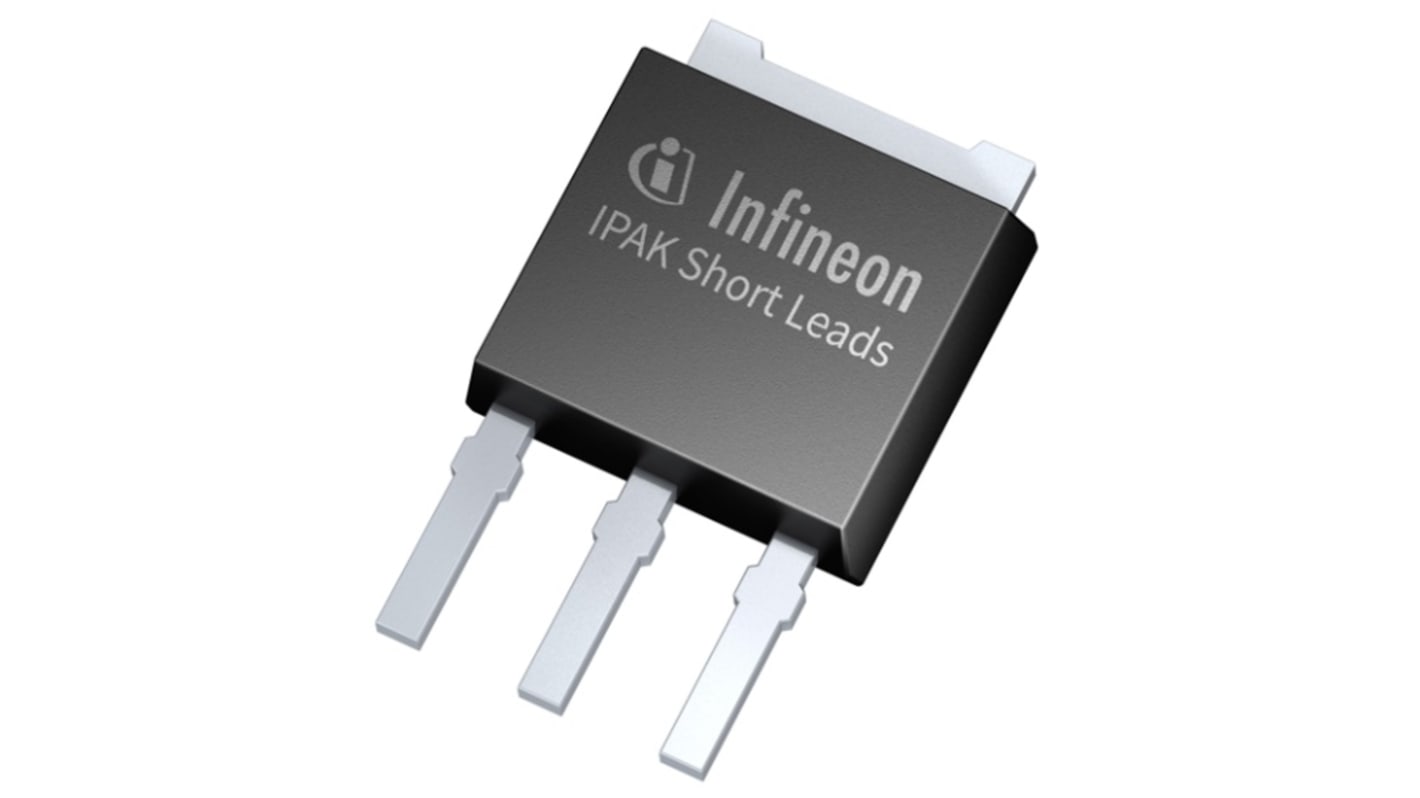
Infineon CoolMOS™ P7 N-Channel MOSFET Transistor & Diode, 7 A, 800 V, 3-Pin IPAK IPS80R750P7AKMA1
- RS Stock No.:
- 220-7441P
- Mfr. Part No.:
- IPS80R750P7AKMA1
- Brand:
- Infineon

Bulk discount available
Subtotal 50 units (supplied in a tube)*
£47.00
(exc. VAT)
£56.50
(inc. VAT)
FREE delivery for orders over £50.00
Temporarily out of stock
- Shipping from 20 August 2026
Need more? Click ‘Check delivery dates’ to find extra stock and lead times.
Units | Per unit |
|---|---|
| 50 - 90 | £0.94 |
| 100 - 240 | £0.90 |
| 250 - 490 | £0.86 |
| 500 + | £0.801 |
*price indicative
- RS Stock No.:
- 220-7441P
- Mfr. Part No.:
- IPS80R750P7AKMA1
- Brand:
- Infineon
Specifications
Technical Reference
Legislation and Compliance
Product Details
Find similar products by selecting one or more attributes.
Select all | Attribute | Value |
|---|---|---|
| Brand | Infineon | |
| Channel Type | N | |
| Maximum Continuous Drain Current | 7 A | |
| Maximum Drain Source Voltage | 800 V | |
| Package Type | IPAK (TO-251) | |
| Series | CoolMOS™ P7 | |
| Mounting Type | Through Hole | |
| Pin Count | 3 | |
| Maximum Drain Source Resistance | 0.75 O | |
| Channel Mode | Enhancement | |
| Maximum Gate Threshold Voltage | 3.5V | |
| Number of Elements per Chip | 1 | |
| Select all | ||
|---|---|---|
Brand Infineon | ||
Channel Type N | ||
Maximum Continuous Drain Current 7 A | ||
Maximum Drain Source Voltage 800 V | ||
Package Type IPAK (TO-251) | ||
Series CoolMOS™ P7 | ||
Mounting Type Through Hole | ||
Pin Count 3 | ||
Maximum Drain Source Resistance 0.75 O | ||
Channel Mode Enhancement | ||
Maximum Gate Threshold Voltage 3.5V | ||
Number of Elements per Chip 1 | ||
The Infineon 800V Cool MOS P7 super junction MOSFET series is a perfect fit for low power SMPS applications by fully addressing market needs in performance, ease-of-use and price/performance ratio. It mainly focuses on fly back applications including adapter and charger, LED driver, audio SMPS, AUX and industrial power. This new product family offers up to 0.6% efficiency gain and 2°C to 8°C lower MOSFET temperature compared to its predecessor as well as to competitor parts tested in typical fly back applications. It also enables higher power density designs through lower switching losses and better DPAK R DS(on) products. Overall, it helps customers save BOM cost and reduce assembly effort.
Best-in-class FOM R DS(on) * E oss
reduced Qg, C is and C oss
Best-in-class DPAK R DS(on) of 280mΩ
Best-in-class V (GS)the of 3V and smallest V (GS)the variation of ± 0.5V
Integrated Zener diode ESD protection up to Class 2 (HBM)
Best-in-class quality and reliability
Fully optimized portfolio
0.1% to 0.6% efficiency gain and 2°C to 8°C lower MOSFET temperature as compared to Cool MOS™ C3
Enabling higher power density designs, BOM savings and lower assembly cost
Easy to drive and to design-in
Better production yield by reducing ESD related failures
Less production issues and reduced field returns
Easy to select right parts for fine tuning of designs