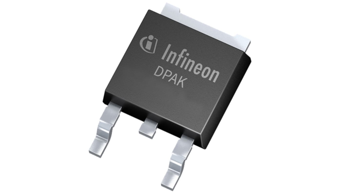
Infineon OptiMOS™ 2 N-Channel MOSFET, 27 A, 100 V, 3-Pin DPAK IPD33CN10NGATMA1
- RS Stock No.:
- 215-2506
- Mfr. Part No.:
- IPD33CN10NGATMA1
- Brand:
- Infineon

Subtotal (1 pack of 20 units)*
£9.58
(exc. VAT)
£11.50
(inc. VAT)
FREE delivery for orders over £50.00
In Stock
- 12,260 unit(s) ready to ship
Need more? Click ‘Check delivery dates’ to find extra stock and lead times.
Units | Per unit | Per Pack* |
|---|---|---|
| 20 + | £0.479 | £9.58 |
*price indicative
- RS Stock No.:
- 215-2506
- Mfr. Part No.:
- IPD33CN10NGATMA1
- Brand:
- Infineon
Specifications
Technical Reference
Legislation and Compliance
Product Details
Find similar products by selecting one or more attributes.
Select all | Attribute | Value |
|---|---|---|
| Brand | Infineon | |
| Channel Type | N | |
| Maximum Continuous Drain Current | 27 A | |
| Maximum Drain Source Voltage | 100 V | |
| Series | OptiMOS™ 2 | |
| Package Type | DPAK (TO-252) | |
| Mounting Type | Surface Mount | |
| Pin Count | 3 | |
| Maximum Drain Source Resistance | 0.033 Ω | |
| Channel Mode | Enhancement | |
| Maximum Gate Threshold Voltage | 4V | |
| Number of Elements per Chip | 1 | |
| Transistor Material | Si | |
Select all | ||
|---|---|---|
Brand Infineon | ||
Channel Type N | ||
Maximum Continuous Drain Current 27 A | ||
Maximum Drain Source Voltage 100 V | ||
Series OptiMOS™ 2 | ||
Package Type DPAK (TO-252) | ||
Mounting Type Surface Mount | ||
Pin Count 3 | ||
Maximum Drain Source Resistance 0.033 Ω | ||
Channel Mode Enhancement | ||
Maximum Gate Threshold Voltage 4V | ||
Number of Elements per Chip 1 | ||
Transistor Material Si | ||
The Infineon's 100V OptiMOS™ power MOSFETs offer superior solutions for high efficiency, high power-density SMPS. Compared to the next best technology this family achieves a reduction of 30% in both R DS(on) and FOM (figure of merit).
N-channel, normal level
Excellent gate charge x R DS(on) product (FOM)
Very low on-resistance R DS(on)
Pb-free lead plating
Qualified according to JEDEC for target application
Ideal for high-frequency switching and synchronous rectification
Excellent gate charge x R DS(on) product (FOM)
Very low on-resistance R DS(on)
Pb-free lead plating
Qualified according to JEDEC for target application
Ideal for high-frequency switching and synchronous rectification