Infineon OptiMOS™ Dual N-Channel MOSFET, 50 A, 25 V, 8-Pin TISON-8 BSG0811NDATMA1
- RS Stock No.:
- 215-2467P
- Mfr. Part No.:
- BSG0811NDATMA1
- Brand:
- Infineon

Subtotal 10 units (supplied on a continuous strip)*
£11.12
(exc. VAT)
£13.34
(inc. VAT)
FREE delivery for orders over £50.00
In Stock
- Plus 8,370 unit(s) shipping from 17 November 2025
Need more? Click ‘Check delivery dates’ to find extra stock and lead times.
Units | Per unit |
|---|---|
| 10 + | £1.112 |
*price indicative
- RS Stock No.:
- 215-2467P
- Mfr. Part No.:
- BSG0811NDATMA1
- Brand:
- Infineon
Specifications
Technical Reference
Legislation and Compliance
Product Details
Find similar products by selecting one or more attributes.
Select all | Attribute | Value |
|---|---|---|
| Brand | Infineon | |
| Channel Type | N | |
| Maximum Continuous Drain Current | 50 A | |
| Maximum Drain Source Voltage | 25 V | |
| Package Type | TISON-8 | |
| Series | OptiMOS™ | |
| Mounting Type | Surface Mount | |
| Pin Count | 8 | |
| Maximum Drain Source Resistance | 0.003 Ω | |
| Channel Mode | Enhancement | |
| Maximum Gate Threshold Voltage | 2V | |
| Transistor Material | Si | |
| Number of Elements per Chip | 2 | |
| Select all | ||
|---|---|---|
Brand Infineon | ||
Channel Type N | ||
Maximum Continuous Drain Current 50 A | ||
Maximum Drain Source Voltage 25 V | ||
Package Type TISON-8 | ||
Series OptiMOS™ | ||
Mounting Type Surface Mount | ||
Pin Count 8 | ||
Maximum Drain Source Resistance 0.003 Ω | ||
Channel Mode Enhancement | ||
Maximum Gate Threshold Voltage 2V | ||
Transistor Material Si | ||
Number of Elements per Chip 2 | ||
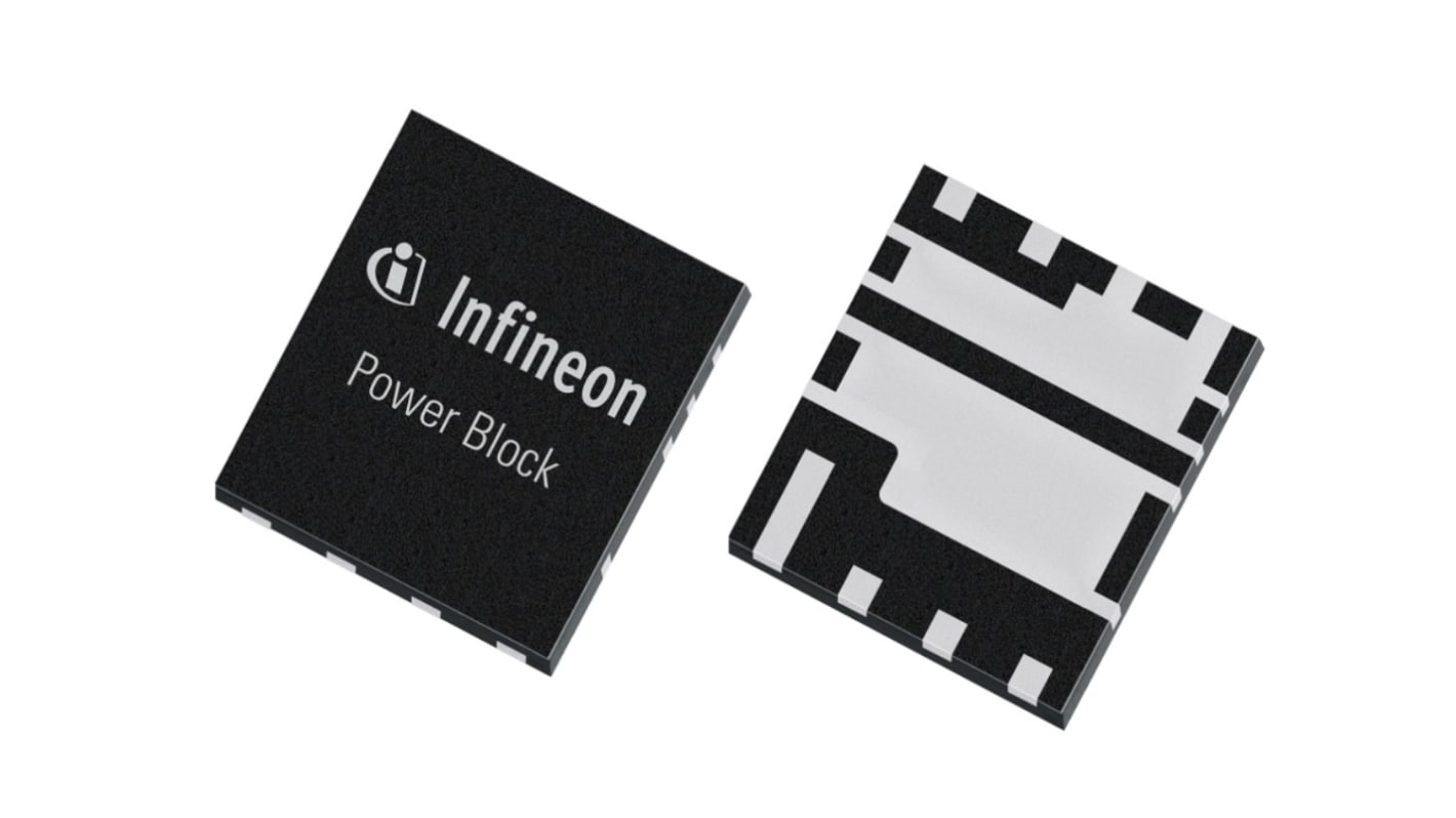
The Infineon OptiMOS™ 5 Power Block is a leadless SMD package in a 5.0x6.0mm² package outline, including a low-side and a high-side MOSFET in a synchronous buck converter configuration. By replacing two separate discrete packages, such as SO8 or SuperSO8, with the OptiMOS™ 5 Power Block, customers can shrink their designs up to 85%. Standardizing power packages benefits the customer, as the number of different package outlines available in the market place is minimized.
50A max average load current
Source-down low side MOSFET for better PCB cooling
Internally connected low-side and high side (lowest loop inductance)
High side Kelvin connection for more efficient driving
Source-down low side MOSFET for better PCB cooling
Internally connected low-side and high side (lowest loop inductance)
High side Kelvin connection for more efficient driving