onsemi N-Channel MOSFET, 24 A, 650 V, 3-Pin D2PAK NVB150N65S3F
- RS Stock No.:
- 195-2518P
- Mfr. Part No.:
- NVB150N65S3F
- Brand:
- onsemi

Subtotal 10 units (supplied on a continuous strip)*
£12.71
(exc. VAT)
£15.25
(inc. VAT)
FREE delivery for orders over £50.00
Last RS stock
- Final 550 unit(s), ready to ship
Units | Per unit |
|---|---|
| 10 + | £1.271 |
*price indicative
- RS Stock No.:
- 195-2518P
- Mfr. Part No.:
- NVB150N65S3F
- Brand:
- onsemi
Specifications
Technical Reference
Legislation and Compliance
Product Details
Find similar products by selecting one or more attributes.
Select all | Attribute | Value |
|---|---|---|
| Brand | onsemi | |
| Channel Type | N | |
| Maximum Continuous Drain Current | 24 A | |
| Maximum Drain Source Voltage | 650 V | |
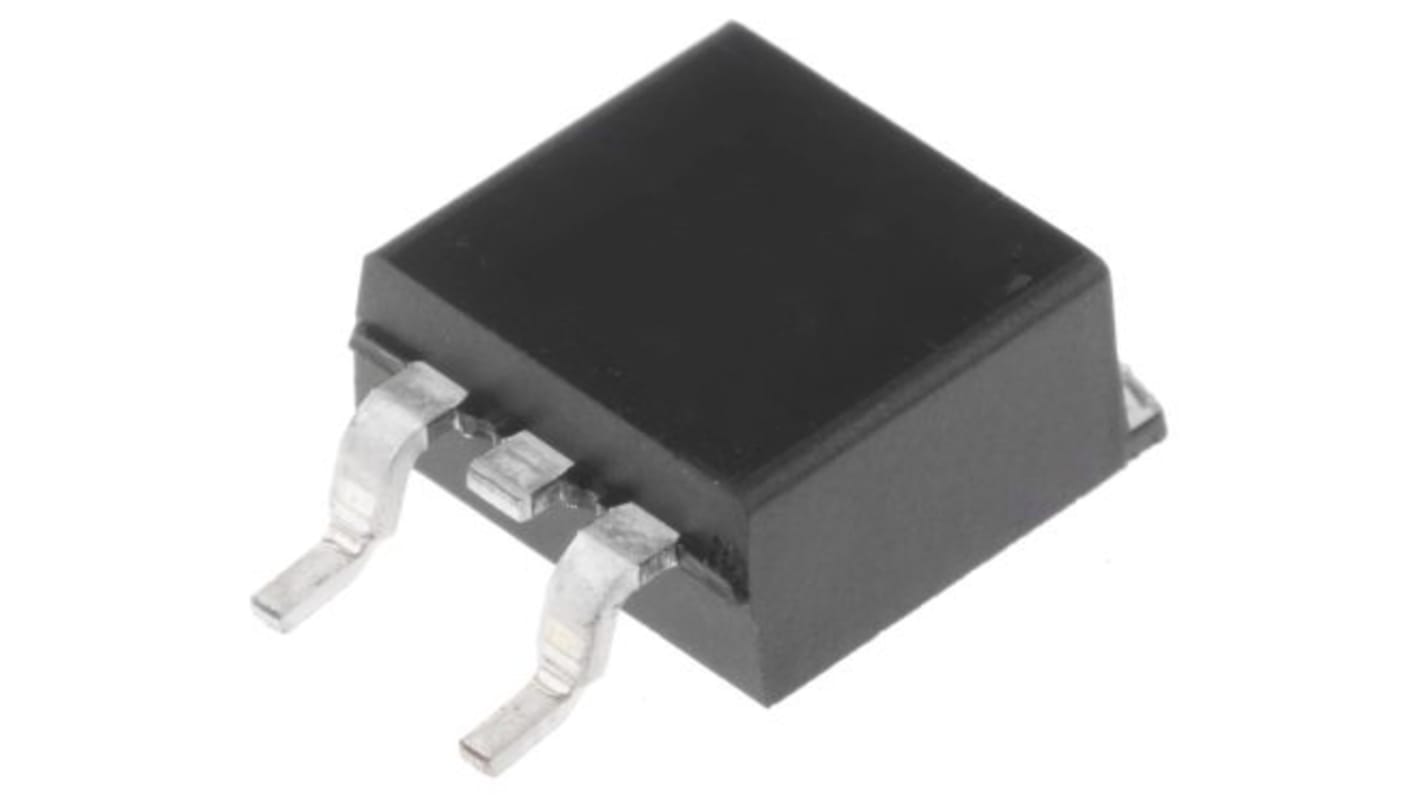
| Package Type | D2PAK (TO-263) | |
| Mounting Type | Surface Mount | |
| Pin Count | 3 | |
| Maximum Drain Source Resistance | 150 mΩ | |
| Channel Mode | Enhancement | |
| Maximum Gate Threshold Voltage | 5V | |
| Minimum Gate Threshold Voltage | 3V | |
| Maximum Power Dissipation | 192 W | |
| Transistor Configuration | Single | |
| Maximum Gate Source Voltage | ±30 V | |
| Width | 9.65mm | |
| Typical Gate Charge @ Vgs | 43 nC @ 10 V | |
| Length | 10.67mm | |
| Number of Elements per Chip | 1 | |
| Maximum Operating Temperature | +150 °C | |
| Minimum Operating Temperature | -55 °C | |
| Forward Diode Voltage | 1.3V | |
| Automotive Standard | AEC-Q101 | |
| Height | 4.58mm | |
| Select all | ||
|---|---|---|
Brand onsemi | ||
Channel Type N | ||
Maximum Continuous Drain Current 24 A | ||
Maximum Drain Source Voltage 650 V | ||
Package Type D2PAK (TO-263) | ||
Mounting Type Surface Mount | ||
Pin Count 3 | ||
Maximum Drain Source Resistance 150 mΩ | ||
Channel Mode Enhancement | ||
Maximum Gate Threshold Voltage 5V | ||
Minimum Gate Threshold Voltage 3V | ||
Maximum Power Dissipation 192 W | ||
Transistor Configuration Single | ||
Maximum Gate Source Voltage ±30 V | ||
Width 9.65mm | ||
Typical Gate Charge @ Vgs 43 nC @ 10 V | ||
Length 10.67mm | ||
Number of Elements per Chip 1 | ||
Maximum Operating Temperature +150 °C | ||
Minimum Operating Temperature -55 °C | ||
Forward Diode Voltage 1.3V | ||
Automotive Standard AEC-Q101 | ||
Height 4.58mm | ||
SUPERFET® III MOSFET is ON Semiconductor’s brand−new high voltage super−junction (SJ) MOSFET family that is utilizing charge balance technology for outstanding low on−resistance and lower gate charge performance. This advanced technology is tailored to minimize conduction loss, provide superior switching performance, and withstand extreme dv/dt rate. Consequently, SUPERFET III MOSFET is very suitable for the various power system for miniaturization and higher efficiency.SUPERFET III FRFET® MOSFET’s optimized reverse recovery performance of body diode can remove additional component and improve system reliability.
701 V @ TJ = 150°C
Typ. RDS(on) = 114 m
Ultra Low Gate Charge (Typ. Qg = 43 nC)
Low Effective Output Capacitance (Typ. Coss(eff.) = 385 pF)
These Devices are Pb−Free
Applications
Automotive On Board Charger
Automotive DC/DC Converter for HEV
Typ. RDS(on) = 114 m
Ultra Low Gate Charge (Typ. Qg = 43 nC)
Low Effective Output Capacitance (Typ. Coss(eff.) = 385 pF)
These Devices are Pb−Free
Applications
Automotive On Board Charger
Automotive DC/DC Converter for HEV