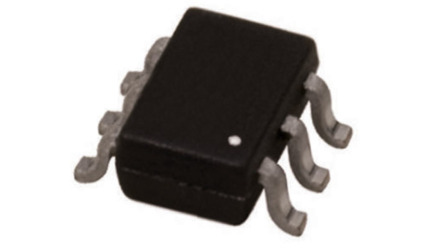
onsemi Dual N-Channel MOSFET, 510 mA, 50 V, 6-Pin SOT-23 NDC7002N
- RS Stock No.:
- 178-7598
- Mfr. Part No.:
- NDC7002N
- Brand:
- onsemi

Subtotal (1 reel of 3000 units)*
£348.00
(exc. VAT)
£417.00
(inc. VAT)
FREE delivery for orders over £50.00
- Plus 6,000 unit(s) shipping from 20 October 2025
Units | Per unit | Per Reel* |
|---|---|---|
| 3000 + | £0.116 | £348.00 |
*price indicative
- RS Stock No.:
- 178-7598
- Mfr. Part No.:
- NDC7002N
- Brand:
- onsemi
Select all | Attribute | Value |
|---|---|---|
| Brand | onsemi | |
| Channel Type | N | |
| Maximum Continuous Drain Current | 510 mA | |
| Maximum Drain Source Voltage | 50 V | |
| Package Type | SOT-23 | |
| Mounting Type | Surface Mount | |
| Pin Count | 6 | |
| Maximum Drain Source Resistance | 4 Ω | |
| Channel Mode | Enhancement | |
| Minimum Gate Threshold Voltage | 1V | |
| Maximum Power Dissipation | 960 mW | |
| Transistor Configuration | Isolated | |
| Maximum Gate Source Voltage | -20 V, +20 V | |
| Transistor Material | Si | |
| Width | 1.7mm | |
| Length | 3mm | |
| Maximum Operating Temperature | +150 °C | |
| Typical Gate Charge @ Vgs | 1 nC @ 10 V | |
| Number of Elements per Chip | 2 | |
| Height | 1mm | |
| Minimum Operating Temperature | -55 °C | |
Select all | ||
|---|---|---|
Brand onsemi | ||
Channel Type N | ||
Maximum Continuous Drain Current 510 mA | ||
Maximum Drain Source Voltage 50 V | ||
Package Type SOT-23 | ||
Mounting Type Surface Mount | ||
Pin Count 6 | ||
Maximum Drain Source Resistance 4 Ω | ||
Channel Mode Enhancement | ||
Minimum Gate Threshold Voltage 1V | ||
Maximum Power Dissipation 960 mW | ||
Transistor Configuration Isolated | ||
Maximum Gate Source Voltage -20 V, +20 V | ||
Transistor Material Si | ||
Width 1.7mm | ||
Length 3mm | ||
Maximum Operating Temperature +150 °C | ||
Typical Gate Charge @ Vgs 1 nC @ 10 V | ||
Number of Elements per Chip 2 | ||
Height 1mm | ||
Minimum Operating Temperature -55 °C | ||
Enhancement Mode Dual MOSFET, Fairchild Semiconductor
ON Semi MOSFETs provide superior design reliability from reduced voltage spikes and overshoot, to lower junction capacitance and reverse recovery charge, to elimination of additional external components to keep systems up and running longer.
