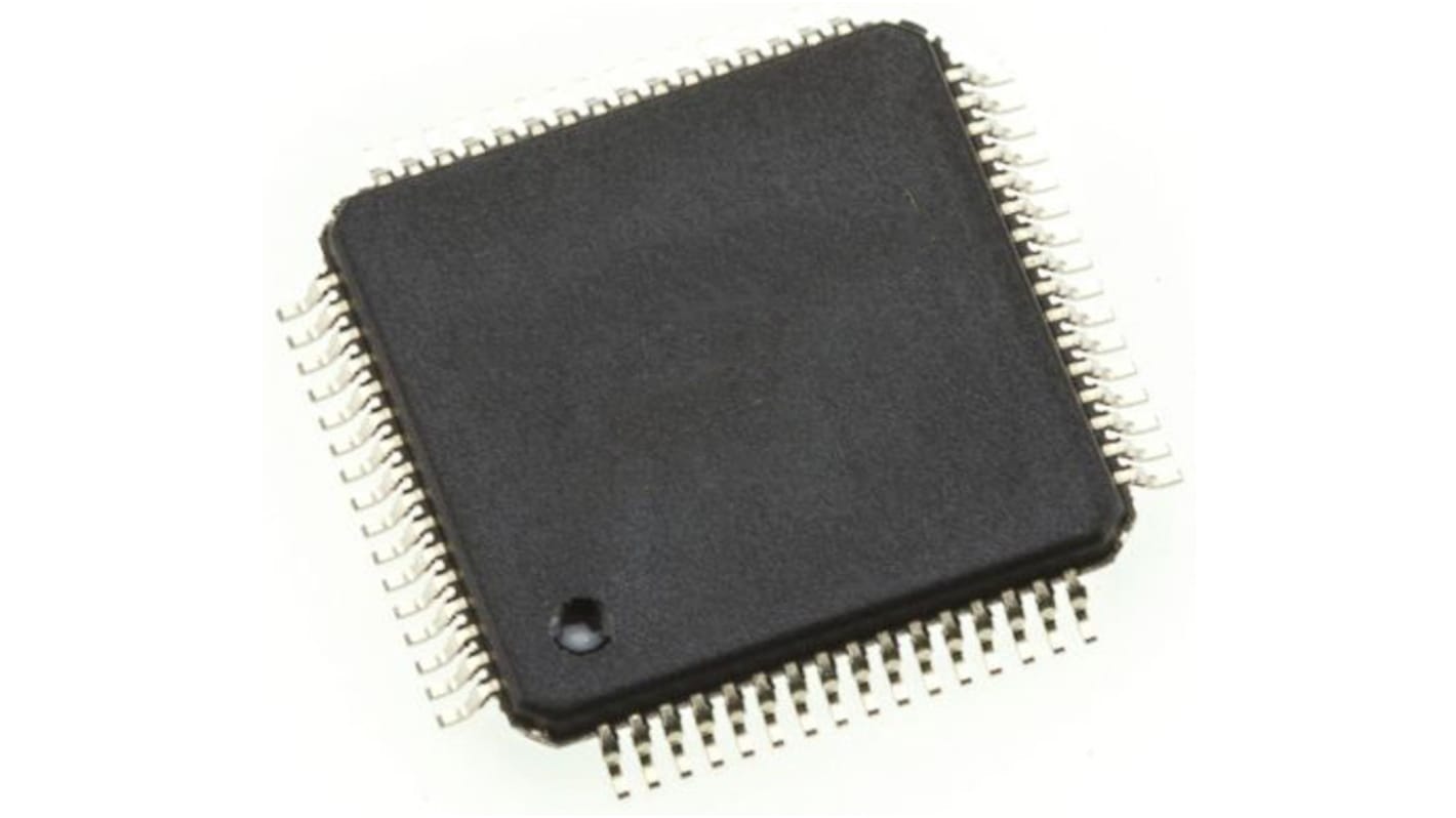
Infineon, 32 bit ARM Cortex M0, CY8C4147 Microcontroller, 48 MHz, 128kB FLASH, 64-Pin TQFP
- RS Stock No.:
- 176-9022P
- Mfr. Part No.:
- CY8C4147AZI-S475
- Brand:
- Infineon

Bulk discount available
View bulk pricing optionsSubtotal 10 units (supplied in a tray)*
£41.20
(exc. VAT)
£49.40
(inc. VAT)
FREE delivery for orders over £60.00
Temporarily out of stock
- Shipping from 09 October 2026
Need more? Click ‘Check delivery dates’ to find extra stock and lead times.
Units | Per unit |
|---|---|
| 10 - 24 | £4.12 |
| 25 - 99 | £3.78 |
| 100 - 249 | £3.67 |
| 250 + | £3.58 |
*price indicative
- RS Stock No.:
- 176-9022P
- Mfr. Part No.:
- CY8C4147AZI-S475
- Brand:
- Infineon
Specifications
Technical Reference
Legislation and Compliance
Product Details
Find similar products by selecting one or more attributes.
Select all | Attribute | Value |
|---|---|---|
| Brand | Infineon | |
| Series | CY8C4147 | |
| Product Type | Microcontroller | |
| Package Type | TQFP | |
| Mount Type | Surface | |
| Pin Count | 64 | |
| Device Core | ARM Cortex M0 | |
| Data Bus Width | 32bit | |
| Program Memory Size | 128kB | |
| Maximum Clock Frequency | 48MHz | |
| RAM Size | 16kB | |
| Maximum Supply Voltage | 5.5V | |
| Minimum Operating Temperature | -40°C | |
| Maximum Operating Temperature | 85°C | |
| Number of Programmable I/Os | 54 | |
| Height | 1.4mm | |
| Length | 10mm | |
| Analogue Comparators | 2 | |
| Width | 10mm | |
| Standards/Approvals | No | |
| Minimum Supply Voltage | 1.71V | |
| Instruction Set Architecture | Thumb-2 | |
| ADCs | 2 x 10/12 Bit | |
| Program Memory Type | FLASH | |
| Number of Timers | 1 | |
| Automotive Standard | No | |
| Select all | ||
|---|---|---|
Brand Infineon | ||
Series CY8C4147 | ||
Product Type Microcontroller | ||
Package Type TQFP | ||
Mount Type Surface | ||
Pin Count 64 | ||
Device Core ARM Cortex M0 | ||
Data Bus Width 32bit | ||
Program Memory Size 128kB | ||
Maximum Clock Frequency 48MHz | ||
RAM Size 16kB | ||
Maximum Supply Voltage 5.5V | ||
Minimum Operating Temperature -40°C | ||
Maximum Operating Temperature 85°C | ||
Number of Programmable I/Os 54 | ||
Height 1.4mm | ||
Length 10mm | ||
Analogue Comparators 2 | ||
Width 10mm | ||
Standards/Approvals No | ||
Minimum Supply Voltage 1.71V | ||
Instruction Set Architecture Thumb-2 | ||
ADCs 2 x 10/12 Bit | ||
Program Memory Type FLASH | ||
Number of Timers 1 | ||
Automotive Standard No | ||
PSoC® 4 is a scalable and reconfigurable platform architecture for a family of programmable embedded system controllers with an Arm® Cortex®-M0 CPU. It combines programmable and reconfigurable analog and digital blocks with flexible automatic routing. The PSoC 4200_BL product family, based on this platform, is a combination of a microcontroller with an integrated Bluetooth Low Energy (BLE), also known as Bluetooth Smart, radio and subsystem (BLESS).
Four opamps with reconfigurable high-drive external and high-bandwidth internal drive, Comparator modes, and ADC input buffering capability Can operate in Deep Sleep mode.
Four programmable logic blocks called universal digital blocks, (UDBs), each with eight macrocells and data path
Cypress-provided peripheral component library, user-defined state machines, and Verilog input
Power Management:
Active mode: 1.7 mA at 3-MHz flash program execution
Deep Sleep mode: 1.5 μA with watch crystal oscillator