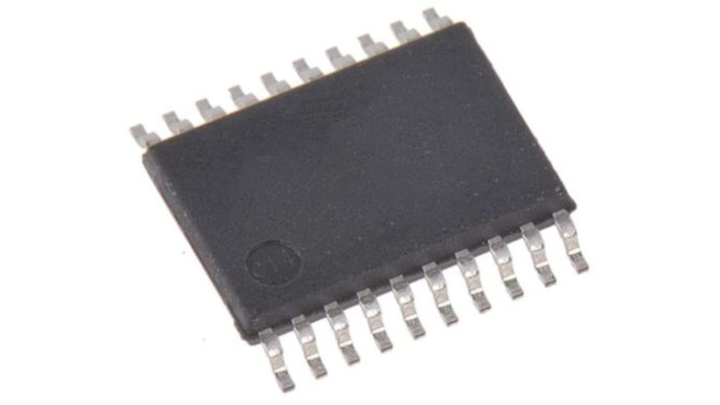
Renesas Electronics 9DB102BGILF, LVDS Buffer 2 TTL Buffer, 20-Pin TSSOP
- RS Stock No.:
- 217-7929P
- Mfr. Part No.:
- 9DB102BGILF
- Brand:
- Renesas Electronics

Bulk discount available
View bulk pricing optionsSubtotal 10 units (supplied in a tube)*
£29.50
(exc. VAT)
£35.40
(inc. VAT)
FREE delivery for orders over £60.00
In Stock
- 45 unit(s) ready to ship
Need more? Click ‘Check delivery dates’ to find extra stock and lead times.
Units | Per unit |
|---|---|
| 10 - 20 | £2.95 |
| 25 - 95 | £2.776 |
| 100 - 245 | £2.418 |
| 250 + | £2.29 |
*price indicative
- RS Stock No.:
- 217-7929P
- Mfr. Part No.:
- 9DB102BGILF
- Brand:
- Renesas Electronics
Specifications
Technical Reference
Legislation and Compliance
Product Details
Find similar products by selecting one or more attributes.
Select all | Attribute | Value |
|---|---|---|
| Brand | Renesas Electronics | |
| Number of Drivers | 2 | |
| Product Type | LVDS Buffer | |
| Input Type | TTL | |
| Sub Type | Buffer | |
| Output Type | Buffer | |
| Number of Elements per Chip | 2 | |
| Mount Type | Surface | |
| Package Type | TSSOP | |
| Pin Count | 20 | |
| Minimum Supply Voltage | 3V | |
| Maximum Supply Voltage | 3.3V | |
| Minimum Operating Temperature | -40°C | |
| ESD Protection | Yes | |
| Maximum Operating Temperature | 85°C | |
| Standards/Approvals | No | |
| Series | 9DB102 | |
| Height | 1.05mm | |
| Length | 6.6mm | |
| Automotive Standard | No | |
| Select all | ||
|---|---|---|
Brand Renesas Electronics | ||
Number of Drivers 2 | ||
Product Type LVDS Buffer | ||
Input Type TTL | ||
Sub Type Buffer | ||
Output Type Buffer | ||
Number of Elements per Chip 2 | ||
Mount Type Surface | ||
Package Type TSSOP | ||
Pin Count 20 | ||
Minimum Supply Voltage 3V | ||
Maximum Supply Voltage 3.3V | ||
Minimum Operating Temperature -40°C | ||
ESD Protection Yes | ||
Maximum Operating Temperature 85°C | ||
Standards/Approvals No | ||
Series 9DB102 | ||
Height 1.05mm | ||
Length 6.6mm | ||
Automotive Standard No | ||
The Renesas Electronics 9DB102 zero-delay buffer supports PCI Express clocking requirements. The 9DB102 is driven by a differential SRC output pair from an IDT CK409/CK410-compliant main clock generator such as the 952601 or 954101. It attenuates jitter on the input clock and has a selectable PLL Band Width to maximize performance in systems with or without Spread- Spectrum clocking.
2 - 0.7 V HCSL differential output pairs
Phase jitter: PCIe Gen2 < 3.1 ps rms
Phase jitter: PCIe Gen1 < 86 ps peak to peak
Supports zero delay buffer mode and fanout mode
Bandwidth programming available
33-110 MHz operation in PLL mode
10-110 MHz operation in Bypass mode