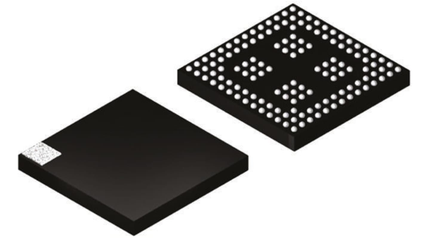
Lattice FPGA iCE40HX8K-CB132, iCE40 HX 7680 Cells, 128kbit, 960 Blocks, 132-Pin csBGA
- RS Stock No.:
- 772-0060
- Mfr. Part No.:
- iCE40HX8K-CB132
- Brand:
- Lattice Semiconductor

Stock information currently inaccessible
- RS Stock No.:
- 772-0060
- Mfr. Part No.:
- iCE40HX8K-CB132
- Brand:
- Lattice Semiconductor
Specifications
Technical Reference
Legislation and Compliance
Find similar products by selecting one or more attributes.
Select all | Attribute | Value |
|---|---|---|
| Brand | Lattice Semiconductor | |
| Family Name | iCE40 HX | |
| Number of Logic Cells | 7680 | |
| Number of Logic Units | 960 | |
| Number of Registers | 7680 | |
| Mounting Type | Surface Mount | |
| Package Type | csBGA | |
| Pin Count | 132 | |
| Number of RAM Bits | 128kbit | |
| Dimensions | 8 x 8 x 1.1mm | |
| Height | 1.1mm | |
| Length | 8mm | |
| Minimum Operating Temperature | -40 °C | |
| Maximum Operating Supply Voltage | 1.26 V | |
| Width | 8mm | |
| Minimum Operating Supply Voltage | 1.14 V | |
| Maximum Operating Temperature | +85 °C | |
| Select all | ||
|---|---|---|
Brand Lattice Semiconductor | ||
Family Name iCE40 HX | ||
Number of Logic Cells 7680 | ||
Number of Logic Units 960 | ||
Number of Registers 7680 | ||
Mounting Type Surface Mount | ||
Package Type csBGA | ||
Pin Count 132 | ||
Number of RAM Bits 128kbit | ||
Dimensions 8 x 8 x 1.1mm | ||
Height 1.1mm | ||
Length 8mm | ||
Minimum Operating Temperature -40 °C | ||
Maximum Operating Supply Voltage 1.26 V | ||
Width 8mm | ||
Minimum Operating Supply Voltage 1.14 V | ||
Maximum Operating Temperature +85 °C | ||