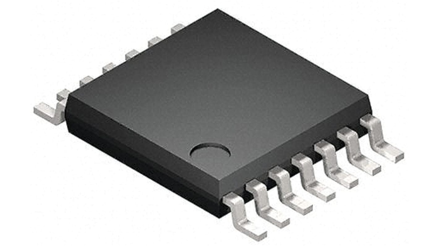
Toshiba 74VHC74FT 2 Flip Flop IC 74VHC, CMOS, 14-Pin TSSOP
- RS Stock No.:
- 171-3463
- Mfr. Part No.:
- 74VHC74FT
- Brand:
- Toshiba

Subtotal (1 pack of 50 units)*
£8.25
(exc. VAT)
£9.90
(inc. VAT)
FREE delivery for orders over £60.00
In Stock
- Plus 550 unit(s) shipping from 04 May 2026
- Plus 6,100 unit(s) shipping from 11 May 2026
Need more? Click ‘Check delivery dates’ to find extra stock and lead times.
Units | Per unit | Per Pack* |
|---|---|---|
| 50 + | £0.165 | £8.25 |
*price indicative
- RS Stock No.:
- 171-3463
- Mfr. Part No.:
- 74VHC74FT
- Brand:
- Toshiba
Specifications
Technical Reference
Legislation and Compliance
Product Details
Find similar products by selecting one or more attributes.
Select all | Attribute | Value |
|---|---|---|
| Brand | Toshiba | |
| Product Type | Flip Flop IC | |
| Logic Family | 74VHC | |
| Input Type | TTL, CMOS | |
| Output Type | CMOS | |
| Clock Frequency | 70MHz | |
| Polarity | Inverting | |
| Mount Type | Surface | |
| Package Type | TSSOP | |
| Minimum Supply Voltage | 2V | |
| Pin Count | 14 | |
| Maximum Supply Voltage | 5.5V | |
| Flip-Flop Type | D Flip-Flop | |
| Maximum Propagation Delay Time @ CL | 12ns | |
| Minimum Operating Temperature | -40°C | |
| Trigger Type | Positive Edge | |
| Number of Elements per Chip | 2 | |
| Maximum Operating Temperature | 125°C | |
| Standards/Approvals | No | |
| Series | 74VHC74FT | |
| Length | 5mm | |
| Height | 1mm | |
| Automotive Standard | AEC-Q100 | |
| Select all | ||
|---|---|---|
Brand Toshiba | ||
Product Type Flip Flop IC | ||
Logic Family 74VHC | ||
Input Type TTL, CMOS | ||
Output Type CMOS | ||
Clock Frequency 70MHz | ||
Polarity Inverting | ||
Mount Type Surface | ||
Package Type TSSOP | ||
Minimum Supply Voltage 2V | ||
Pin Count 14 | ||
Maximum Supply Voltage 5.5V | ||
Flip-Flop Type D Flip-Flop | ||
Maximum Propagation Delay Time @ CL 12ns | ||
Minimum Operating Temperature -40°C | ||
Trigger Type Positive Edge | ||
Number of Elements per Chip 2 | ||
Maximum Operating Temperature 125°C | ||
Standards/Approvals No | ||
Series 74VHC74FT | ||
Length 5mm | ||
Height 1mm | ||
Automotive Standard AEC-Q100 | ||
The 74VHC74FT is an advanced high speed CMOS D-FLIP FLOP fabricated with silicon gate C2MOS technology. It achieves the high speed operation similar to equivalent Bipolar Schottky TTL while maintaining the CMOS low power dissipation. The signal level applied to the D INPUT is transferred to Q OUTPUT during the positive going transition of the CK pulse. CLR and PR are independent of the CK and are accomplished by setting the appropriate input low. An input protection circuit ensures that 0 to 5.5 V can be applied to the input pins without regard to the supply voltage. This device can be used to interface 5 V to 3 V systems and two supply systems such as battery back up. This circuit prevents device destruction due to mismatched supply and input voltages.
Wide operating temperature range: Topr = -40 to 125
High speed: fMAX = 185 MHz (typ.) at VCC = 5.0 V
Low power dissipation: ICC = 4.0 μA (max) at Ta = 25
High noise immunity: VNIH = VNIL = 28 % VCC (min)
Power-down protection is provided on all inputs.
Balanced propagation delays: tPLH ≈ tPHL
Wide operating voltage range: VCC(opr) = 2.0 V to 5.5 V
Low noise: VOLP = 1.0 V (max)
Pin and function compatible with the 74 series (74AC/HC/AHC/LV etc.) 74 type
Related links
- Toshiba 2 Flip Flop IC 74VHC 14-Pin TSSOP
- Toshiba 2 Flip Flop IC 74HC 14-Pin SOIC
- Toshiba 74HC74D 2 Flip Flop IC 74HC 14-Pin SOIC
- Nexperia 74HCT74D 2 Flip Flop IC HCT 14-Pin SOIC
- Toshiba 74LCX74FT Dual D Type Flip Flop IC 14-Pin TSSOP
- onsemi MC14013BDR2G 2 Flip Flop IC 4000 CMOS, 14-Pin SOIC
- onsemi MC14013BDG 2 Flip Flop IC 4000 CMOS, 14-Pin SOIC
- onsemi 2 Flip Flop IC 4000 CMOS, 14-Pin SOIC